A battery pack bidirectional equalization charging and discharging circuit and its charging and discharging control implementation method
A technology for balancing charging and discharging, and battery packs, which is applied in secondary battery charging/discharging, battery circuit devices, circuit devices, etc. It can solve problems such as insufficient charging, battery over-discharging, and battery overcharging to improve conversion efficiency. The circuit structure is simple and the effect of improving the circuit gain
- Summary
- Abstract
- Description
- Claims
- Application Information
AI Technical Summary
Problems solved by technology
Method used
Image
Examples
Embodiment 1
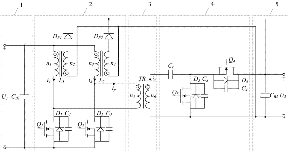
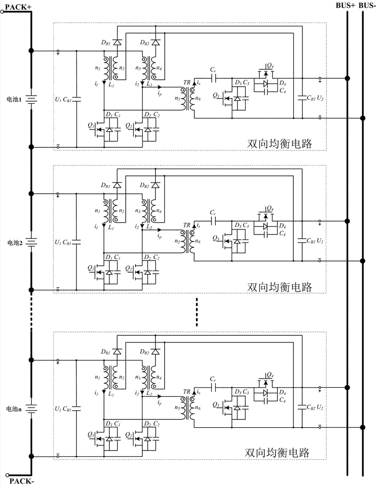
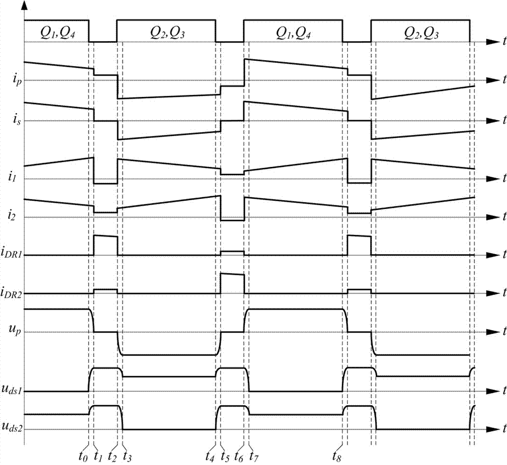
[0026] Utilizing the charging and discharging control method of the battery pack bidirectional equalizing charging and discharging circuit, the first switching unit includes a coupling inductor L 1 , L 2 , containing anti-parallel body diode D 1 , output junction capacitance C 1 The switching tube Q 1 and contains anti-parallel body diode D 2 , output junction capacitance C 2 The switching tube Q 2 ; Coupled inductance L 1 The primary winding n 1 The dotted end of the coupled inductor L 2 The primary winding n 3 The end of the same name is connected, the switch tube Q 1 The source and switch Q 2 connected to the source, the coupled inductor L 1 The primary winding n 1 The opposite end and the switching tube Q 1 connected to the drain, the coupled inductor L 2 The primary winding n 3 The opposite end and the switching tube Q 2 connected to the drain, the coupled inductor L 1 The secondary winding n 2 The opposite side of the coupled inductor L 2 The secondary...
Embodiment 2
[0065] Utilizing the charging and discharging control method of the battery pack bidirectional equalizing charging and discharging circuit, the first switching unit includes a coupling inductor L 1 , L 2 , containing anti-parallel body diode D 1 , output junction capacitance C 1 The switching tube Q 1 and contains anti-parallel body diode D2 , output junction capacitance C 2 The switching tube Q 2 ; Coupled inductance L 1 The primary winding n 1 The dotted end of the coupled inductor L 2 The primary winding n 3 The end of the same name is connected, the switch tube Q 1 The source and switch Q 2 connected to the source, the coupled inductor L 1 The primary winding n 1 The opposite end and the switching tube Q 1 connected to the drain, the coupled inductor L 2 The primary winding n 3 The opposite end and the switching tube Q 2 connected to the drain, the coupled inductor L 1 The secondary winding n 2 The opposite side of the coupled inductor L 2 The secondary w...
PUM
 Abstract
Description
Claims
Application Information


