Epitaxial structure of GaSb group infrared laser having electron barrier layer

A technology of electron blocking layer and epitaxial structure, which is applied in the direction of lasers, phonon exciters, laser components, etc., can solve the problems of increased room temperature threshold current of lasers, increased device internal loss, waste of epitaxial materials, etc., to reduce crystal defects , Guarantee the performance of the device and avoid the effect of loss

Inactive Publication Date: 2016-01-27
CHANGCHUN UNIV OF SCI & TECH
View PDF0 Cites 7 Cited by
  • Summary
  • Abstract
  • Description
  • Claims
  • Application Information

AI Technical Summary

Problems solved by technology

However, too many wells will not only cause waste of epitaxial materials, but also increase the internal loss of the device, which wi

Method used


Image

  • Epitaxial structure of GaSb group infrared laser having electron barrier layer
  • Epitaxial structure of GaSb group infrared laser having electron barrier layer
  • Epitaxial structure of GaSb group infrared laser having electron barrier layer

Examples


Embodiment Construction

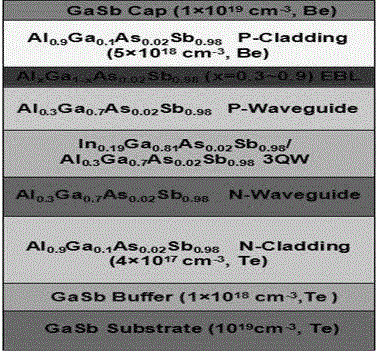
[0026] described in the present invention one An epitaxial structure of a GaSb-based mid-infrared semiconductor laser with an electron-blocking layer, comprising a GaSb substrate, a buffer layer, an n-type confinement layer, a lower waveguide layer, an active region, an upper waveguide layer, an electron-blocking layer, and a p-type confinement layer and cover layer.

[0027] The above-mentioned buffer layer is a material equal to or close to the lattice constant of the substrate material, such as GaSb, AlSb, etc.; the above-mentioned n-type confinement layer, lower waveguide layer, upper waveguide layer, electron blocking layer, and p-type confinement layer can be connected with the substrate Matching materials, such as AlGaAsSb, AlInGaAsSb, etc.; the above-mentioned active region is an InGaAsSb / AlGaAsSbI type quantum well, a GaAsSb / GaAsII type quantum well or an InAs / (In)GaSb gap type quantum well.

[0028] The above-mentioned electron blocking layer is non-doped, and the ...


PUM


Abstract

The present invention provides an epitaxial structure of a GaSb group infrared laser having an electron barrier layer, and relates to the field of the semiconductor laser epitaxial technology. The epitaxial structure provided by the invention comprises a GaSb substrate, a buffer layer, a n-type limitation layer, a n-type ducting layer, an active region, a p-type ducting layer, an electron barrier layer and p-type limitation layer. The electron barrier layer is arranged between the p-type ducting layer and the p-type limitation layer, and the conduction band potential of the electron barrier layer is higher than the conduction band potential of the p-type limitation layer. Compared with the prior art, the epitaxial structure of a GaSb group infrared laser having an electron barrier layer may reduce the Auger recombination in a quantum well, restrain the overflow of the conduction band electrons in the quantum well to the p-type limitation layer, and effectively improve the performance of the GaSb group infrared semiconductor laser.

Description

technical field [0001] The invention relates to the technical field of semiconductor laser epitaxy, in particular to an epitaxial structure of a GaSb-based mid-infrared semiconductor laser with an electron blocking layer. Background technique [0002] GaSb-based mid-infrared semiconductor lasers have important applications in the fields of medical care, laser optical communication, lidar and trace gas monitoring, and have attracted widespread attention. By adjusting the In composition in the quantum well material InGaAsSb in the active region, the luminescence wavelength can cover the spectral range from 1.3 μm (GaAsSb) to far-infrared 12 μm (InAsSb). For lasers in this band, Auger recombination is likely to occur in the quantum well of the active region. The leakage of high-energy carriers in the confinement layer caused by Auger recombination is the main factor affecting the threshold current and characteristic temperature of the laser. At the same time, compared with ot...

Claims


Application Information

Patent Timeline
IPC IPC(8): H01S5/343
Inventor 安宁刘国军刘超李占国刘鹏程何斌太常量马晓辉席文星
Owner CHANGCHUN UNIV OF SCI & TECH
Why Eureka
Try Eureka