
A Manufacturing Technology of 40v Schottky Diode with Reduced Secondary Breakdown Ratio

A Schottky diode, secondary breakdown technology, applied in semiconductor/solid-state device manufacturing, semiconductor devices, electrical components, etc. The effect of increasing junction depth and uniformity and increasing impurity concentration

Active Publication Date: 2019-04-30
TIANSHUI TIANGUANG SEMICON
View PDF3 Cites 0 Cited by
  • Summary
  • Abstract
  • Description
  • Claims
  • Application Information

AI Technical Summary

Problems solved by technology

[0007] Disadvantages of this process: the secondary breakdown rate is 30%-100% higher, the Schottky breakdown curve is poor, and the reliability is poor during the use of the device
[0008] The Schottky diodes currently used in the main process have thin epitaxial thickness, low implanted doping concentration, low annealing temperature resulting in shallow junctions, uneven push junctions, high secondary breakdown ratios, and poor Schottky breakdown curves.

Method used

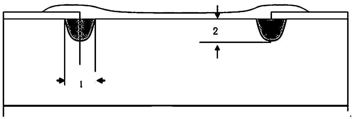
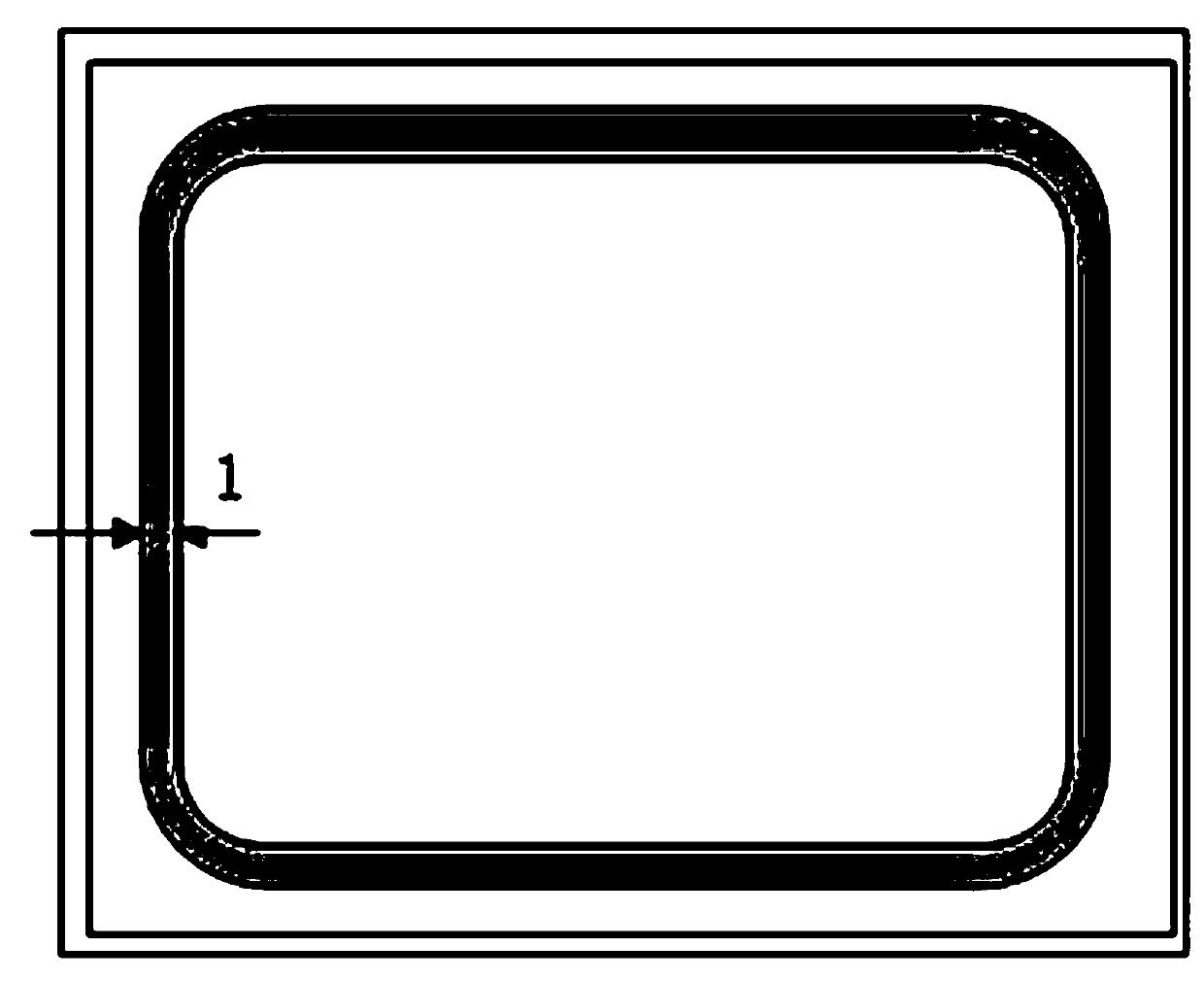
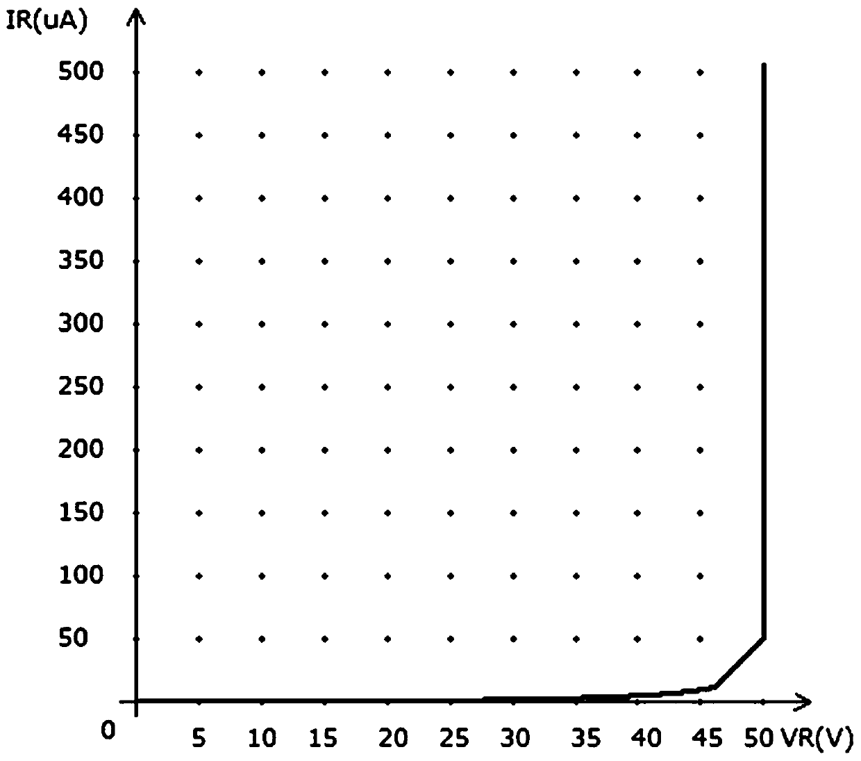

Image

  • A Manufacturing Technology of 40v Schottky Diode with Reduced Secondary Breakdown Ratio
  • A Manufacturing Technology of 40v Schottky Diode with Reduced Secondary Breakdown Ratio
  • A Manufacturing Technology of 40v Schottky Diode with Reduced Secondary Breakdown Ratio

Examples


Embodiment 1

[0035] A 40V Schottky diode manufacturing process (only applied to 40V) that reduces the secondary breakdown ratio. The steps are:

[0036] a. Substrate silicon wafer cleaning: substrate silicon wafers are cleaned with NH 3 h 2 O:H 2 o 2 :H 2 O=1:1:5 cleaning solution and HCL:H 2 o 2 :H 2 O = 1:1:5 cleaning solution at 75°C for 10 minutes each, rinse the substrate wafers with water for 10 minutes, and dry them before use;

[0037] b. Initial oxidation: The substrate silicon wafer that has completed step a is subjected to the initial oxidation process. First, put the silicon wafer into a quartz boat, and then enter the boat into the quartz furnace tube. The boat speed is 20cm / s. After the boat enters, cover the grinding port. Nitrogen was introduced at 750°C, 6 liters per minute, for 30 minutes, the temperature was raised from 750°C to 950°C, and the temperature was kept at 950°C. Stop nitrogen and change to oxygen. After 10 minutes of oxygen, change to oxygen and hydrog...

Embodiment 2

[0059] A 40V Schottky diode manufacturing process (only applied to 40V) that reduces the secondary breakdown ratio. The steps are:

[0060] a. Substrate silicon wafer cleaning: substrate silicon wafers are cleaned with NH 3 h 2 O:H 2 o 2 :H 2 O=1:1:5 cleaning solution and HCL:H 2 o 2 :H 2 O = 1:1:5 cleaning solution at 70°C for 9 minutes each, rinse the substrate wafer with water for 9 minutes, and dry it for later use;

[0061] b. Initial oxidation: The substrate silicon wafer that has completed step a is subjected to the initial oxidation process. First, put the silicon wafer into a quartz boat, and then enter the boat into the quartz furnace tube. The boat speed is 19cm / s. After the boat enters, cover the grinding port. Nitrogen was fed at 747°C, 5 liters per minute, 29 minutes, the temperature rose from 747°C to 947°C, and the temperature was kept at 947°C. Stop nitrogen and change to oxygen. After 9 minutes of oxygen, change to oxygen and hydrogen for hydrogen Oxy...

Embodiment 3

[0083] A 40V Schottky diode manufacturing process (only applied to 40V) that reduces the secondary breakdown ratio. The steps are:

[0084] a. Substrate silicon wafer cleaning: substrate silicon wafers are cleaned with NH 3 h 2 O:H 2 o 2 :H 2 O=1:1:5 cleaning solution and HCL:H 2 o 2 :H 2 O = 1:1:5 cleaning solution at 80°C for 11 minutes each, rinse the substrate wafer with water for 1 minute, and dry it before use;

[0085] b. Initial oxidation: The substrate silicon wafer that has completed step a is subjected to the initial oxidation process. First, put the silicon wafer into a quartz boat, and then enter the boat into the quartz furnace tube. The boat speed is 21cm / s. After entering the boat, cover the grinding port. Nitrogen was fed at 753°C, 7 liters per minute, 31 minutes, the temperature rose from 753°C to 953°C, and the temperature was kept at 953°C. Stop nitrogen and change to oxygen. After 11 minutes of oxygen, change to oxygen and hydrogen for hydrogen Oxy...


PUM


Abstract

The invention provides a 40 V Schottky diode manufacturing process capable of reducing the secondary breakdown ratio. The Schottky diode manufacturing process includes the main step of setting epitaxy parameters of a silicon wafer, wherein the epitaxy thickness is 5.2-5.4 micrometers, the resistivity is 0.84-0.92 omega. cm, the initial oxidation parameter is 5000-7000 a, the implantation dose is 2E-3E+15, and the annealing temperature is 1070-1080 DEG C. According to the 40 V Schottky diode manufacturing process, the high ion implantation dose of 2E-3E+15 is adopted, so that the impurity concentration of PN junctions is increased; meanwhile, the high annealing temperature is adopted, so that the junction depth of a device is increased, and the uniformity of the device is improved; the larger the dosage concentration and the junction depth are, the stronger the voltage withstanding capability of the device will be. The Schottky diode is a surface shallow junction device, the secondary breakdown ratio is reduced to 5% or below, a Schottky breakdown curve is good, and the device has high reliability in the use process.

Description

technical field [0001] The invention relates to the technical field of diode technology, in particular to a manufacturing technology of a 40V Schottky diode with reduced secondary breakdown ratio. Background technique [0002] The main manufacturing process of Schottky diodes currently used: [0003] ① The silicon wafer epitaxy parameters are set to be thin, generally (epitaxy thickness: 4.6-5.1 um resistivity 0.84-0.92Ω.cm) [0004] ② Initial oxidation 5000-7000À [0005] ③ Injection dose 5E+14-1.5E+15 [0006] ④ Annealing 1050-1060℃ [0007] Disadvantages of this process: the secondary breakdown rate is 30%-100% higher, the Schottky breakdown curve is poor, and the reliability is poor during the use of the device. [0008] The Schottky diodes currently used are mainly thin in epitaxial thickness, low in doping concentration, and low annealing temperature resulting in shallow junctions and uneven push junctions, resulting in high secondary breakdown ratios and poor Scho...

Claims


Application Information

Patent Timeline
IPC IPC(8): H01L21/329H01L21/265H01L21/324H01L29/872
CPCH01L21/265H01L21/324H01L29/66143H01L29/872
Inventor 张晓情杜林德
Owner TIANSHUI TIANGUANG SEMICON
Learn More