Circuit board for replacing golden metal strips and manufacturing method of circuit board

A manufacturing method and circuit board technology, which are applied in the directions of printed circuit components, electrical connection printed components, etc., can solve the problems of low reliability and high manufacturing cost of gold fingers, and achieve high application reliability, low manufacturing cost, and improved wear resistance. performance effect

Inactive Publication Date: 2016-02-24
QUZHOU SUNLORD CIRCUIT BOARD CO LTD
View PDF8 Cites 6 Cited by
  • Summary
  • Abstract
  • Description
  • Claims
  • Application Information

AI Technical Summary

Problems solved by technology

[0004] The above scheme strengthens the protection of metal by passivating the reactivity of the metal. Although the corrosion resistance of the gold finger is improved to a certain extent, this scheme still cannot fundamentally solve the problem of high manufacturing cost and low reliability of the gold finger. question

Method used


Image

  • Circuit board for replacing golden metal strips and manufacturing method of circuit board
  • Circuit board for replacing golden metal strips and manufacturing method of circuit board

Examples


Embodiment 1

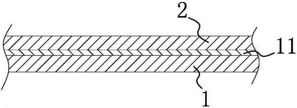
[0031] Such as figure 1 As shown, the circuit board manufacturing method used to replace gold fingers includes the following steps: A, pretreating the semi-finished circuit board 1 after solder masking; B, performing alloy electroplating on the semi-finished circuit board 1 after completing the pretreatment so that at least one layer of alloy layer 2 is formed on the surface of the copper layer 11 of the plug-in connection position of the semi-finished circuit board 1, and the alloy layer 2 is composed of chemical elements copper and chemical elements zinc, tin, nickel, cobalt, chromium, silver, gold , iron, lead, platinum, rhodium, palladium, indium at least one composition, then the semi-finished circuit board 1 after alloy electroplating is washed; The finished circuit board is made, preferably, the alloy layer 2 here can be any one of the chemical element copper and the chemical element zinc, tin, nickel, cobalt, chromium, silver, gold, iron, lead, platinum, rhodium, palla...

Embodiment 2

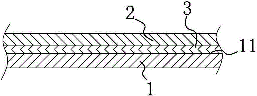
[0037] Such as figure 2 As shown, the structure, principle and implementation steps of this embodiment are similar to those of Embodiment 1, the difference is that, when the alloy layer 2 is electroplated, an intermediate layer 3 can be provided between the copper layer 11 and the alloy layer 2, And the intermediate layer 3 is composed of any one or more of the chemical elements nickel, tin and zinc, that is, the electroplating of the alloy layer 2 can be directly plated on the copper layer 11, or other elements can be plated on the surface of the copper layer 11. Metals, such as nickel, tin, zinc, etc., are then plated with the alloy layer 2 on the surfaces of these metals.


PUM

PropertyMeasurementUnit
thicknessaaaaaaaaaa
electrical resistivityaaaaaaaaaa
hardnessaaaaaaaaaa

Abstract

The invention relates to a circuit board for replacing golden metal strips and a manufacturing method of the circuit board. The circuit board solves the technical problem that golden metal strips of an existing circuit board are high in cost. The method includes the following steps that firstly, a semi-finished circuit board obtained after resistance welding is pretreated; secondly, alloy electroplating is conducted on the pretreated semi-finished circuit board, at least one alloy layer is formed on the surface of a copper layer of the plug-pull connection position of the semi-finished circuit board, and then semi-finished circuit board obtained after alloy electroplating is washed through water; and thirdly, the electroplated semi-finished circuit board is polish-brushed and dried, so that the finished circuit board is obtained. The circuit board has the beneficial effects that the plug-pull connection position of the circuit board is electroplated with the alloy-plated layer; and under the condition of meeting contact resistance, the oxidation resistance and corrosion resistance of products are improved remarkably compared with a gold finger circuit board, wear resistance is improved remarkably, the application reliability of the products is higher, and manufacturing cost is lower.

Description

technical field [0001] The invention belongs to the technical field of circuit board processing and manufacturing, and in particular relates to a circuit board for replacing golden fingers and a manufacturing method thereof. Background technique [0002] The gold finger design is widely used in circuit boards with pluggable contact conduction. It requires gold fingers to have strong oxidation and corrosion resistance, high wear resistance and low contact resistance. In the existing gold finger circuit board manufacturing technology, nickel-gold electroplating is generally carried out in the surface treatment process after the solder mask is completed. With the wider and deeper application of golden finger circuit boards in medical, security, aviation and other fields, more stringent requirements are put forward for the reliability of golden finger circuit boards. At present, the reliability and corrosion resistance of the application are usually enhanced by increasing the ...

Claims


Application Information

Patent Timeline
Patent Type & Authority Applications(China)
IPC IPC(8): C25D7/00H05K1/11
Inventor 石林国白耀文胡斐
Owner QUZHOU SUNLORD CIRCUIT BOARD CO LTD
Why Eureka
Try Eureka