Three-dimensional semiconductor device and manufacturing method thereof

A device manufacturing method and semiconductor technology, applied in semiconductor devices, electrical solid devices, electrical components, etc., can solve the problems of large threshold voltage and poor control, and achieve the effect of improving channel current and overcoming current bottlenecks.

Active Publication Date: 2018-09-18
INST OF MICROELECTRONICS CHINESE ACAD OF SCI
View PDF5 Cites 2 Cited by
  • Summary
  • Abstract
  • Description
  • Claims
  • Application Information

AI Technical Summary

Problems solved by technology

In addition, the threshold voltage of the dummy cell will be due to the asymmetric fringe electric field (Fringe Field, such as figure 1 Arrow) will make the threshold voltage too large, difficult to control

Method used


Image

  • Three-dimensional semiconductor device and manufacturing method thereof
  • Three-dimensional semiconductor device and manufacturing method thereof
  • Three-dimensional semiconductor device and manufacturing method thereof

Examples


Embodiment Construction

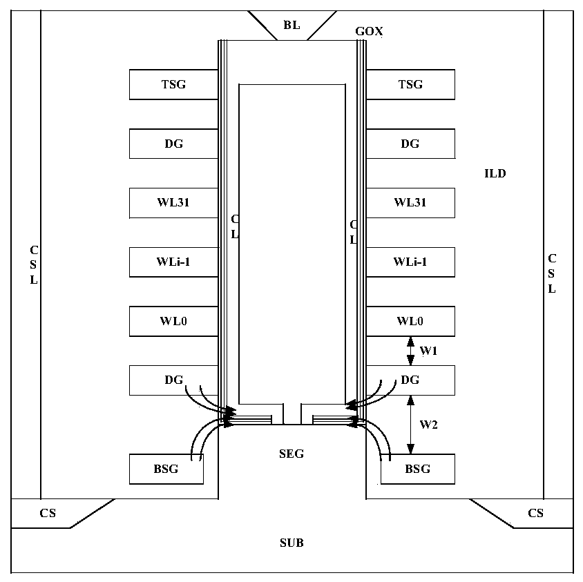
[0022] The features and technical effects of the technical solution of the present invention will be described in detail below with reference to the accompanying drawings and in conjunction with schematic embodiments, and a semiconductor memory device and its manufacture that effectively overcome the current bottleneck, increase the channel current, and effectively control the consistency of the threshold voltage are disclosed. method. It should be pointed out that similar reference numerals represent similar structures, and the terms first, second, upper, lower, etc. used in this application can be used to modify various device structures or manufacturing processes. These modifications do not imply spatial, sequential or hierarchical relationships of the modified device structures or fabrication processes unless specifically stated.

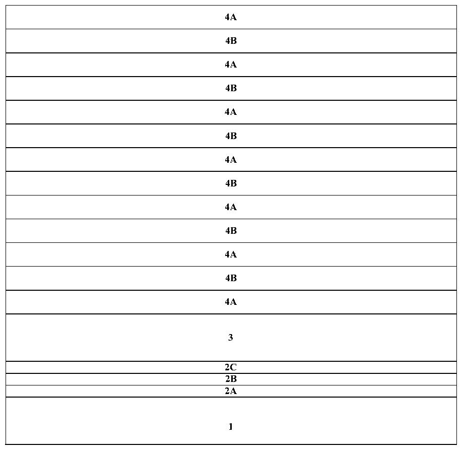
[0023] Such as Figure 2A As shown, a first insulating layer stack 2 (including a lower layer 2A, a middle layer 2B, and an upper layer 2C), a...


PUM


Abstract

A three-dimensional semiconductor device comprising a plurality of memory cells, each comprising: a channel layer distributed along a direction perpendicular to a substrate surface; a bottom gate conductive layer located in a first insulating layer stack and distributed on the side of the channel layer On the wall; the floating gate layer is located on the first insulating layer stack and distributed on the sidewall of the channel layer; a plurality of second insulating layers and a plurality of gate conductive layers are located on the floating gate layer and along the channel Layer sidewalls are stacked alternately; the gate dielectric layer is distributed on the sidewalls of the channel layer; the drain is located on the top of the channel layer; and the source is located in the substrate between two adjacent storage units of multiple storage units . The non-extracted floating gate is embedded inside, and the voltage is induced on the floating gate through the coupling of the voltage on the adjacent extraction gate to assist in completing the channel inversion of the contact area between the SEG and the polysilicon, thereby overcoming the current bottleneck in this area and increasing the channel current. Effectively control the threshold voltage consistency of the floating gate adjacent FETs.

Description

technical field [0001] The invention relates to a semiconductor device and a manufacturing method thereof, in particular to a three-dimensional semiconductor storage device and a manufacturing method thereof. Background technique [0002] In order to improve the density of memory devices, the industry has made extensive efforts to develop methods of reducing the size of two-dimensionally arranged memory cells. As the size of memory cells in two-dimensional (2D) memory devices continues to shrink, signal collisions and interference can increase significantly, making it difficult to perform multi-level cell (MLC) operations. In order to overcome the limitations of 2D memory devices, the industry has developed memory devices with a three-dimensional (3D) structure to increase integration density by three-dimensionally arranging memory cells on a substrate. [0003] Specifically, as figure 1 As shown, a multi-layer stack structure (for example, multiple ONO structures alternat...

Claims


Application Information

Patent Timeline
Patent Type & Authority Patents(China)
IPC IPC(8): H01L27/11521H01L27/11551H01L29/423
CPCH01L29/42324H10B41/00H10B43/35H10B43/27
Inventor 霍宗亮叶甜春
Owner INST OF MICROELECTRONICS CHINESE ACAD OF SCI
Why Eureka
Try Eureka