GaN-enhanced MOSFET formed based on digital wet grating etching technology and preparation method

An enhanced and technical technology, applied in semiconductor/solid-state device manufacturing, semiconductor devices, electrical components, etc., can solve problems such as surface morphology degradation, ion damage, and difficulty in controlling the thickness of AlGaN in the gate area, so as to achieve good morphology and avoid Effects of damage, increased electron mobility, and maximum drain current density

Inactive Publication Date: 2016-11-23
PEKING UNIV
View PDF1 Cites 7 Cited by
  • Summary
  • Abstract
  • Description
  • Claims
  • Application Information

AI Technical Summary

Problems solved by technology

[0005] Among them, the gate etching technology usually uses dry etching technology and plasma treatment, which will cause ion damage in the active region, resulting in degradation of surface morphology and low channel mobility; at the same time, it is difficult to control dry etching rate, making it difficult to control the thickness of the gate AlGaN
Therefore, the common dry etching gate technology based on ICP or RIE will affect the stability and reliability of the device.

Method used


Image

  • GaN-enhanced MOSFET formed based on digital wet grating etching technology and preparation method
  • GaN-enhanced MOSFET formed based on digital wet grating etching technology and preparation method
  • GaN-enhanced MOSFET formed based on digital wet grating etching technology and preparation method

Examples


Embodiment Construction

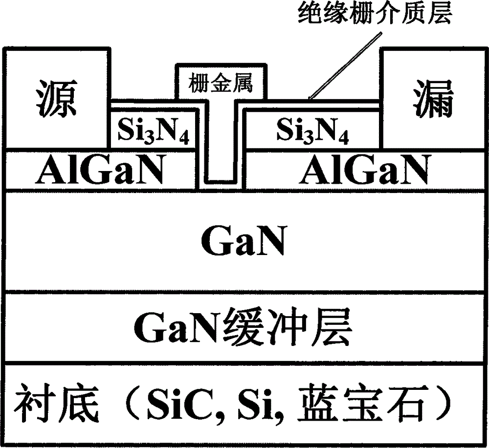
[0026] The schematic diagram of the basic structure of the enhancement mode GaN MOSFET device of the present invention is as figure 1 As shown, it belongs to the metal-oxide-semiconductor field effect transistor. Compared with the enhanced GaN HEMT or MOSFET of the common gate etching technology, the feature of the present invention is that the wet etching technology is used instead of the commonly used plasma dry method. Etching greatly reduces the plasma damage of the gate groove, retains a good surface morphology of the gate groove, and ensures the consistency of the threshold voltage and realizes a high-performance GaN-enhanced MOSFET, wherein the gate metal is the following conductive material A combination of one or more of: platinum, iridium, nickel, gold, molybdenum, palladium, selenium, beryllium, TiN, polysilicon, ITO, the material of the insulating gate dielectric layer is any one of the following materials: Si 3 N 4 、Al 2 o 3 , AlN, HfO 2 , SiO 2 , HfTiO, Sc ...


PUM


Abstract

The invention provides a GaN-enhanced MOSFET formed based on a digital wet grating etching technology and a preparation method, and relates to the field of power electronic devices and high-efficiency power switches of wide-band-gap compound semiconductor materials. The GaN-enhanced MOSFET comprises a substrate, a GaN buffer layer, GaN, AlGaN, an etching mask dielectric layer and an insulated gate dielectric layer from bottom to top; a gate area is defined on the surface of a wafer; the etching mask dielectric layer below the gate area is etched away and the AlGaN layer is etched away by a wet process; and a source region and a drain region are arranged on the surface of the AlGaN to form a source and a drain respectively. The GaN-enhanced MOSFET has the beneficial effects that a gate trench area is etched by the wet process, so that the plasma damage is avoided, the surface shape and form of a gate trench are relatively good, the maximum leakage current density is improved, and the consistency of the grating etching depth and the threshold voltage can be controlled. The developed high-performance wet etching-based GaN-enhanced device can be used for the high-efficiency power switch and an RF power device.

Description

technical field [0001] The invention relates to the field of power electronic devices and high-efficiency power switches of wide-bandgap compound semiconductor materials. Background technique [0002] The characteristics of GaN materials are as follows: (1) Compared with the band gap of Si (1.12eV) and GaAs (1.42eV), the band gap of GaN is 3.4eV, which enables the device to work at high voltage, and also ensures The device will not fail under certain high temperature environment. (2) GaN material has excellent anti-breakdown characteristics, and the breakdown field strength is about 3MV / cm, which is 10 times that of Si material. (3) The GaN material has a high electron saturation drift rate, so devices working under high electric fields still have high electron mobility, and thus obtain high current density, which is very attractive for high-power devices. (4) GaN material also has the characteristics of large dielectric constant, high thermal conductivity, and strong radi...

Claims


Application Information

Patent Timeline
Patent Type & Authority Applications(China)
IPC IPC(8): H01L29/78H01L29/10H01L29/423H01L21/28H01L21/336
Inventor 王茂俊王野陶明郝一龙
Owner PEKING UNIV
Why Eureka
Try Eureka