

Single crystal silicon growth control method
A technology of growth control and single crystal silicon, which is applied in the direction of single crystal growth, single crystal growth, crystal growth, etc., can solve the problems of reducing production efficiency, reducing the quality of supercrystals, and reducing the length of silicon single crystal rods, etc.
- Summary
- Abstract
- Description
- Claims
- Application Information
AI Technical Summary
Problems solved by technology
Method used
Image

Examples
Embodiment 1
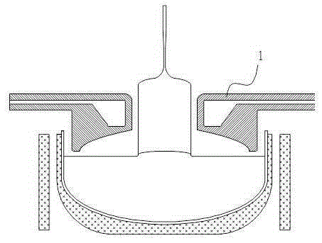
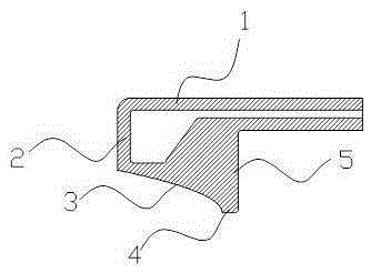
[0020] The long diameter is an 8-inch monocrystalline silicon rod, and the inner diameter is a 22-inch (560mm inner diameter) quartz crucible. The height of the erected surface 2 in the reflection and cooling device is 250 mm, and the surface roughness is controlled at 8-10 μm by shot blasting. The plasma vapor deposition method is used to coat the silicon carbide porous ceramic coating on the surface. The thickness of the coating is 2.42 μm, the inner pore size of the coating is controlled at 1.2 μm-1.5 μm, and the density is greater than 65%. The vertical surface 2 is 20mm away from the side surface of the single crystal silicon rod.
[0021] The semi-parabolic arc segment 3 has an opening of the parabola facing the ingot, the opening height is 130 mm, and the arc segment 3 has a length of 130 mm. The length of the horizontal section 4 is 20mm. The distance between the vertical section 5 and the crucible wall is 10 mm. The semi-parabolic arc section 3, horizontal section ...
Embodiment 2
[0026] The long diameter is an 8-inch single crystal silicon rod, and the inner diameter is a 24-inch (610mm inner diameter) quartz crucible. The height of the erected surface 2 in the reflection and cooling device is 250 mm, and the surface roughness is controlled at 8-10 μm by shot blasting. The plasma vapor deposition method is used to coat the silicon carbide porous ceramic coating on the surface. The thickness of the coating is 2.42 μm, the inner pore size of the coating is controlled at 1.2 μm-1.5 μm, and the density is greater than 65%. The vertical surface 2 is 20mm away from the side surface of the single crystal silicon rod.
[0027] The semi-parabolic arc segment 3, the opening of the parabola faces the ingot, the opening height is 130 mm, and the length of the arc segment 3 is 155 mm. The length of the horizontal section 4 is 20mm. The distance between the vertical section 5 and the crucible wall is 10 mm. The semi-parabolic arc section 3, horizontal section 4 a...
Embodiment 3
[0030]The long diameter is 12 inches (diameter 305) single crystal silicon rod, and the inner diameter is 26 inches (inner diameter 660mm) quartz crucible. The height of the erected surface 2 in the reflection and cooling device is 250 mm, and the surface roughness is controlled at 8-10 μm by shot blasting. The plasma vapor deposition method is used to coat the silicon carbide porous ceramic coating on the surface. The thickness of the coating is 2.42 μm, the inner pore size of the coating is controlled at 1.2 μm-1.5 μm, and the density is greater than 65%. The vertical surface 2 is 20mm away from the side surface of the single crystal silicon rod.
[0031] The semi-parabolic arc section 3, the opening of the parabola faces the ingot, the opening height is 150mm, and the length of the arc section 3 is 125mm. The length of the horizontal section 4 is 20mm. The distance between the vertical section 5 and the crucible wall is 10mm. The semi-parabolic arc section 3, horizontal ...
PUM
| Property | Measurement | Unit |
|---|---|---|
| Thickness | aaaaa | aaaaa |
| Thickness | aaaaa | aaaaa |
| The inside diameter of | aaaaa | aaaaa |
Abstract
Description
Claims
Application Information