Backscattered electron receiving sensor and observation system for electron beam processing process

A technology of backscattered electrons and receiving sensors, which is applied in the direction of instruments, circuits, discharge tubes, etc., can solve problems such as image distortion, affecting observation accuracy, and sensor electrical signal saturation, so as to improve flexibility and automation and reduce labor intensity. Effect

Active Publication Date: 2016-03-16
AVIC BEIJING AERONAUTICAL MFG TECH RES INST
View PDF5 Cites 5 Cited by
  • Summary
  • Abstract
  • Description
  • Claims
  • Application Information

AI Technical Summary

Problems solved by technology

The disadvantage of this technology is that during the working process of large beam current, the secondary electron receiving sensor is easily polluted by metal vapor, which affects the observation accuracy
[0008] The above-mentioned German observation system based on backscattered electron imaging technology can only work in the workplace with a small beam current of a few mA. In the workplace with a large beam current, such as large-thickness electron beam welding or rapid manufacturing of electron beam fuses, the electrical signal saturation of the sensor will occur. , image distortion
However, the observation system based on backscattered electron imaging technology developed by Ukraine has the disadvantages that the image can hardly be seen in the workplace with small beam current, and the definition is not high in the workplace with large beam current.
Existing observation devices based on backscattered electron beam imaging technology are difficult to adapt to all beam working ranges, so that a variety of observation methods must be used in vacuum electron beam processing devices to ensure processing quality

Method used


Image

  • Backscattered electron receiving sensor and observation system for electron beam processing process
  • Backscattered electron receiving sensor and observation system for electron beam processing process
  • Backscattered electron receiving sensor and observation system for electron beam processing process

Examples


Embodiment Construction

[0061] The following will clearly and completely describe the technical solutions in the embodiments of the present invention with reference to the accompanying drawings in the embodiments of the present invention. Obviously, the described embodiments are only some, not all, embodiments of the present invention. Based on the embodiments of the present invention, all other embodiments obtained by persons of ordinary skill in the art without making creative efforts belong to the protection scope of the present invention.

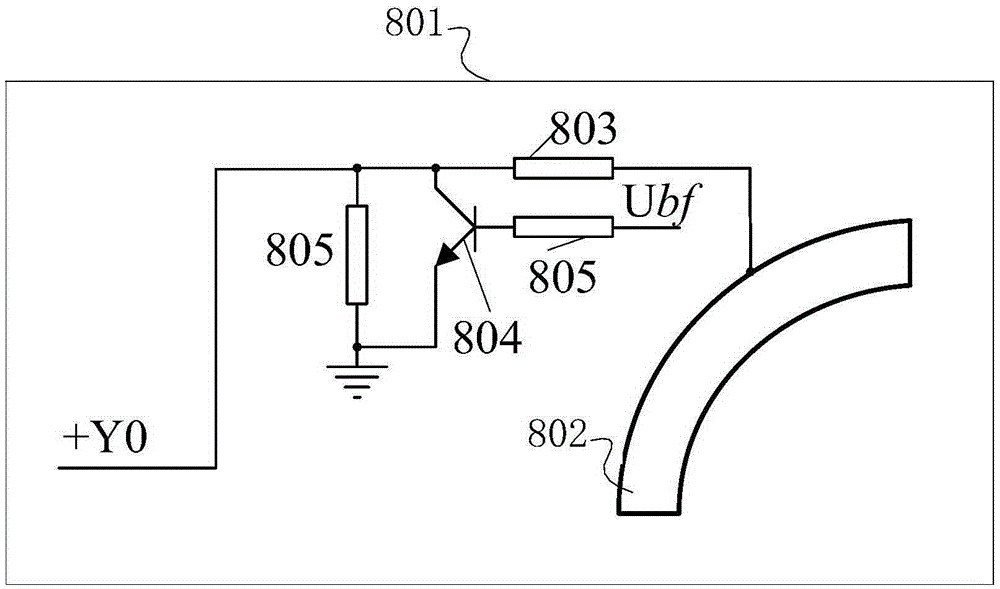
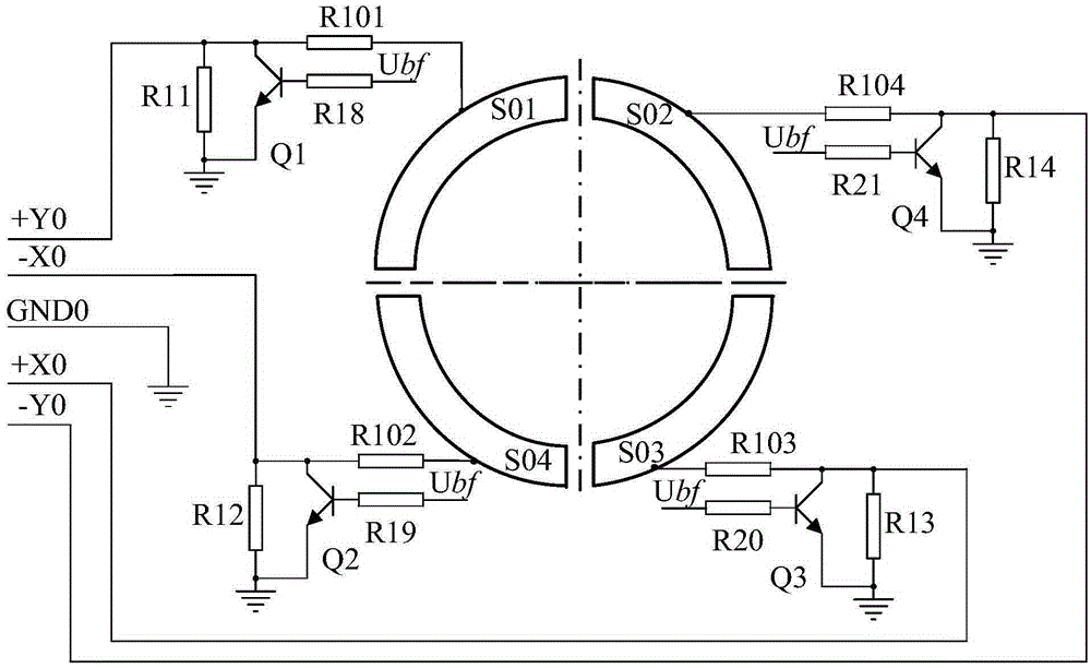
[0062] In view of the fact that the current vacuum electron beam observation technology is difficult to adapt to the characteristics of all beam working ranges, in order to improve the electron beam processing quality, operational flexibility, convenience and automation, a novel design idea is adopted to invent a Observation system based on backscattered electron imaging technology for all beam working ranges. Specifically, it is an observation device that can...


PUM


Abstract

The invention provides a backscattered electron receiving sensor and an observation system for an electron beam processing process. The backscattered electron receiving sensor comprises a sensor assembly, wherein the sensor assembly comprises an electron receiving pole plate, a current-limiting resistor, a transistor, a drive resistor and a sampling resistor; the electron receiving pole plate is connected with one end of the current-limiting resistor; a collector of the transistor is connected with the other end of the current-limiting resistor; an emitter of the transistor is grounded; the sampling resistor is connected between the collector and the emitter of the transistor in parallel; and a base of the transistor is connected with an external beam feedback adjusting circuit through the drive resistor. According to the backscattered electron receiving sensor, an electron beam feedback signal is used for adjusting a maximum voltage amplitude output by the backscattered electron receiving sensor as a control signal, so that the operation flexibility and automatic degree in the processing process of a vacuum electron beam processing device are improved.

Description

technical field [0001] The present invention relates to the technical field of electronic processing, in particular to an observation device for electron beams, specifically a backscattered electron receiving sensor and an observation system for electron beam processing. Background technique [0002] Electron beam processing technology has been widely used in various fields of national economic production, among which vacuum electron beam processing technology is the most widely used. In order to obtain good electron beam processing quality, ordinary optical observation devices and industrial CCDs have been introduced into vacuum electron beam processing technology. in the processing device. [0003] To obtain a clear observation effect with ordinary optical observation devices, it is necessary to consider the optical path design during the electron gun manufacturing process. Usually the light is emitted from the backlight, and through a reflector 1 at a certain angle with ...

Claims


Application Information

Patent Timeline
Patent Type & Authority Applications(China)
IPC IPC(8): H01J37/244G01N23/203
CPCG01N23/203H01J37/244
Inventor 许海鹰邢一思左从进
Owner AVIC BEIJING AERONAUTICAL MFG TECH RES INST
Why Eureka
Try Eureka