Low off-state current tunneling field effect transistor

A tunneling field effect and off-state current technology, applied in circuits, electrical components, semiconductor devices, etc., can solve the problem of limited improvement of TFET performance, and achieve improved performance, low sub-threshold swing, and off-state current suppression. Effect

Inactive Publication Date: 2016-03-16
XIANGTAN UNIV
View PDF1 Cites 8 Cited by
  • Summary
  • Abstract
  • Description
  • Claims
  • Application Information

AI Technical Summary

Problems solved by technology

[0003] Improve the sub-threshold performance of TFET by designing more effective lateral tunneling or vertical tunneling or both, or by using narrow bandgap semiconductor materials (such as III-V InAs, or two-dimensional

Method used


Image

  • Low off-state current tunneling field effect transistor
  • Low off-state current tunneling field effect transistor
  • Low off-state current tunneling field effect transistor

Examples


Embodiment Construction

[0016] The present invention will be further described below in conjunction with the accompanying drawings and embodiments.

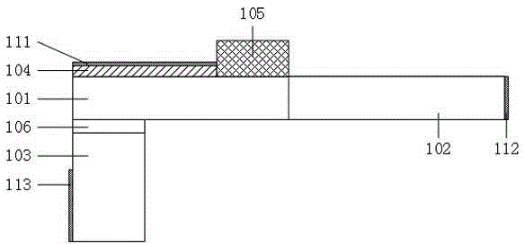
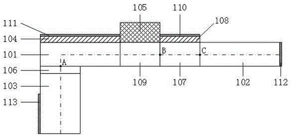
[0017] Such as figure 2 As shown, the present invention includes a channel region 101, a drain region 102, a source region 103, a first gate dielectric layer 104, an isolation region 105, a heavily doped source region 106, an adjustment region 107, and a transition region 109. The channel region 101 adopts n-type indium arsenide (InAs) with a concentration of 5E17cm -3 , the channel region 101 is provided with a first gate dielectric layer 104, and the first gate dielectric layer 104 is made of silicon dioxide (SiO 2 ), the first gate dielectric layer 104 is provided with a first gate 111, the source region 103 is located below the channel region 101 and close to the lower part of the channel region 101, and the source region 103 is made of p-type gallium antimonide (GaSb ), the concentration is 4E18cm -3 , the source region 103 is provided with a s...


PUM


Abstract

The invention discloses a low off-state current tunneling field effect transistor, comprises a source region, a channel region, a drain region and a first gate dielectric layer, wherein the channel region is provided with the first gate dielectric layer, the first gate dielectric layer is provided with a first grid, the source region is arranged under the channel region and close to the lower part of the channel region, the source region is provided with a source electrode, the drain region is arranged at one side of the channel region, a drain electrode is arranged at the right end of the drain region, an adjusting region is arranged between the channel region and the drain region, a transition region is arranged between the channel region and the adjusting region, a second gate dielectric layer is arranged on the adjusting region and is provided with a second grid, the first grid and the second grid are connected together through a lead to function as the grid of the whole field effect transistor, and an isolation region is arranged on the transition region. Since the adjusting region is introduced between the channel region and the drain region, the equivalent resistance of the adjusting region functions so that the low off-state current tunneling field effect transistor can obtain lower subthreshold swing and quiescent dissipation, thus improving the performance of the low off-state current tunneling field effect transistor.

Description

technical field [0001] The invention relates to a field effect transistor, in particular to a low off-state current tunneling field effect transistor. Background technique [0002] With the continuous development of integrated circuit technology and the continuous reduction of device feature size, the traditional metal-oxide-semiconductor field effect transistor (MOSFET, Metal-oxide-semiconductor FieldEffect Transistor) is limited by hot electron injection, making the sub-threshold swing SS (SubthresholdSwing) must not be lower than the limit value of 60mV / decade, which hinders the further shrinking of the device, and in the process, power consumption has gradually become an important factor for primary consideration. Tunneling Field Effect Transistor (TFET, Tunneling Field Effect Transistor) utilizes the band-to-band tunneling (BTBT, Band-to-band Tunneling) mechanism, and the subthreshold swing can be lower than 60mV / decade. Replace traditional MOSFET. [0003] Improve th...

Claims


Application Information

Patent Timeline
IPC IPC(8): H01L29/739H01L29/10H01L29/08
CPCH01L29/7391H01L29/0895H01L29/1033
Inventor 唐明华钟兴宏
Owner XIANGTAN UNIV
Why Eureka
Try Eureka