Optical film, method for producing optical film, and surface light-emitting body
An optical film and manufacturing method technology, applied in chemical instruments and methods, optics, optical components, etc., can solve the problem of inability to take out the outside, and achieve the effects of excellent light extraction efficiency, low curling, and excellent weather resistance.
- Summary
- Abstract
- Description
- Claims
- Application Information
AI Technical Summary
Problems solved by technology
Method used
Image

Examples
Embodiment 1
[0337] (manufacturing of optical films)
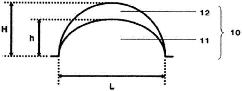
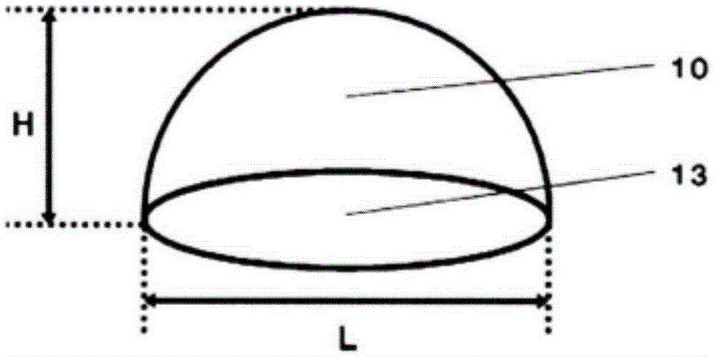
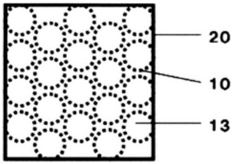
[0338] As the active energy ray-curable composition A for constituting the region α, the active energy ray-curable composition (1) was used, and as the active energy ray-curable composition B for constituting the region β, the active energy ray-curable composition (1) was used. Composition (2), utilize Figure 6 The shown apparatus performs step A (coating including making the active energy ray-curable composition B conform to the surface of the concave-shaped microlens transfer part), step X, step B, step C, and step D in order to manufacture Optical film. Regarding the obtained microlenses of the optical film, the region α is formed of the resin composition A, the region β is formed of the resin composition B, and the average longest diameter L of the bottom portion of the microlens is ave 50μm, the average height of the microlens H ave is 25 μm, the average height h of the region α ave It is 18 μm, and is a spherical sectional m...
Embodiment 2、 comparative example 3~4
[0352] The optical film was obtained in the same manner as in Example 1 except that the region α and the region β of the optical film were formed of the resin composition shown in Table 2.
[0353] Table 2 shows the results of the adhesion test, curl test and friction test of the obtained optical film.
[0354] Table 2
[0355]
Embodiment 3
[0356] [Example 3, Comparative Example 1, 5]
[0357] The optical film was obtained in the same manner as in Example 1 except that the region α and the region β of the optical film were formed of the resin composition shown in Table 3.
[0358] Table 3 shows the results of the adhesion test, curl test and resistivity test of the obtained optical film.
[0359] table 3
[0360]
PUM
| Property | Measurement | Unit |
|---|---|---|
| surface resistance | aaaaa | aaaaa |
| thickness | aaaaa | aaaaa |
| thickness | aaaaa | aaaaa |
Abstract
Description
Claims
Application Information