Conducting film manufacturing method, touch control panel manufacturing method, and touch control panel

A production method and touch panel technology, which are applied in the manufacture of cables/conductors, conductive layers on insulating carriers, circuits, etc., to achieve the effects of reduced material usage, improved light transmittance, and low cost

Active Publication Date: 2016-03-30
TPK TOUCH SOLUTIONS (XIAMEN) INC
View PDF11 Cites 45 Cited by
  • Summary
  • Abstract
  • Description
  • Claims
  • Application Information

AI Technical Summary

Problems solved by technology

[0007] In order to overcome the technical problem of making touch panels by replacing ITO with existing nano-silver wires as new conduc

Method used


Image

  • Conducting film manufacturing method, touch control panel manufacturing method, and touch control panel
  • Conducting film manufacturing method, touch control panel manufacturing method, and touch control panel
  • Conducting film manufacturing method, touch control panel manufacturing method, and touch control panel

Examples


Embodiment Construction

[0064] In order to make the purpose, technical solutions and advantages of the present invention more clear, the present invention will be further described in detail below in conjunction with the accompanying drawings and implementation examples. It should be understood that the specific embodiments described here are only used to explain the present invention, not to limit the present invention.

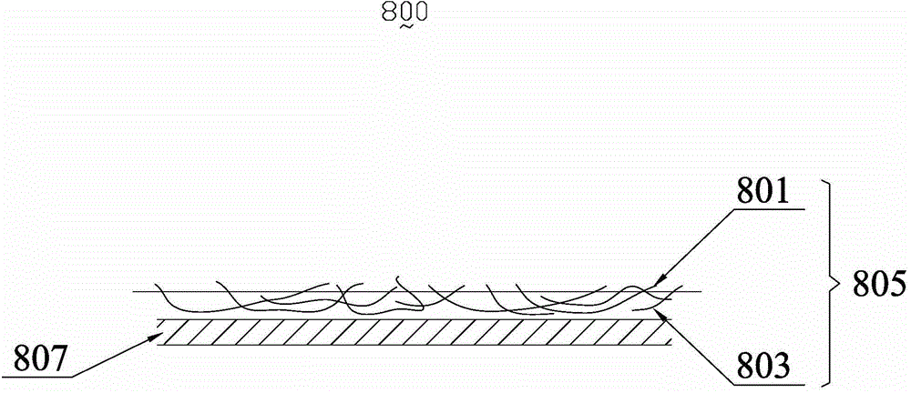
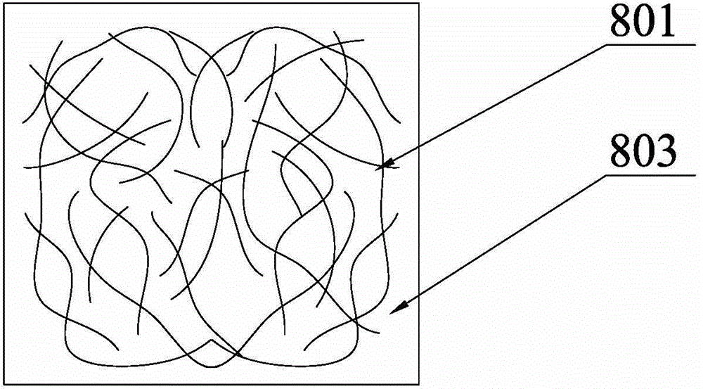
[0065] see figure 1 and figure 2 , is a cross-sectional schematic diagram of the silver nano wire conductive film 800, the silver nano wire film 805 is generally made on the substrate 807, including a plurality of silver nano wires 801 embedded in the matrix 803, and the silver nano wires 801 are arranged on the substrate 803 overlap each other to form a conductive network. The silver nanowires 801 (silvernanowires, SNW for short) have a wire length of 10 μm-300 μm, preferably 20 μm-100 μm, and preferably a length of 20 μm-50 μm, and the diameter (or line width) of the silver na...


PUM

PropertyMeasurementUnit
Line lengthaaaaaaaaaa
Wire diameteraaaaaaaaaa
Depthaaaaaaaaaa

Abstract

The invention relates to the technical field of touch control, and especially relates to a conducting film manufacturing method, a touch control panel manufacturing method, and a touch control panel. The conducting film manufacturing method comprises the steps: S1, providing a transparent base material; S2, coating the transparent base material with a photoresist layer; S3, manufacturing a groove with the corresponding pattern on the photoresist layer, and solidifying the photoresist layer with ultraviolet light; S4, coating the interior of the groove with nano silver thread solution; S5, solidifying the nano silver thread solution in the groove, so as to form a nano silver thread conducting film.

Description

【Technical field】 [0001] The invention relates to the field of touch technology, in particular to a method for manufacturing a conductive film, a method for manufacturing a touch panel, and the touch panel. 【Background technique】 [0002] In capacitive touch panels of traditional smartphones, such as iphone, the material of the conductive film is usually indium tin oxide (referred to as ITO). ITO has high light transmittance and good conductivity, and is widely used as a conductive electrode material for touch panels and display panels. However, indium is an expensive metal material. Using ITO as the material of the conductive layer greatly increases the cost of the touch screen. Moreover, in the patterning process of the ITO conductive layer, the entire surface of the plated ITO film needs to be processed. Etching to form ITO patterns. In this process, a large amount of ITO is etched away, resulting in a large amount of precious metal waste and pollution, and the cost is h...

Claims


Application Information

Patent Timeline
IPC IPC(8): H01B13/00H01B5/14G06F3/041G06F3/044
Inventor 黄松建李绍王硕汶郑太狮
Owner TPK TOUCH SOLUTIONS (XIAMEN) INC
Why Eureka
Try Eureka