Method for forming fin field effect transistor

A fin-type field effect and transistor technology, which is applied in the manufacture of semiconductor/solid-state devices, electrical components, circuits, etc., can solve the problems such as the performance of stress source/drain region needs to be improved, so as to reduce the generation of defects, enhance the activity, and ensure the growth environment Effect

Active Publication Date: 2016-03-30
SEMICON MFG INT (SHANGHAI) CORP
View PDF4 Cites 11 Cited by
  • Summary
  • Abstract
  • Description
  • Claims
  • Application Information

AI Technical Summary

Problems solved by technology

[0006] However, the performance of the stress source/d

Method used


Image

  • Method for forming fin field effect transistor
  • Method for forming fin field effect transistor
  • Method for forming fin field effect transistor

Examples


Embodiment Construction

[0034] As mentioned in the background art, the performance of forming stress source / drain regions in the fins of the prior art fin field effect transistors still needs to be improved. For example, the formed stress source / drain regions have lattice defects and poor uniformity.

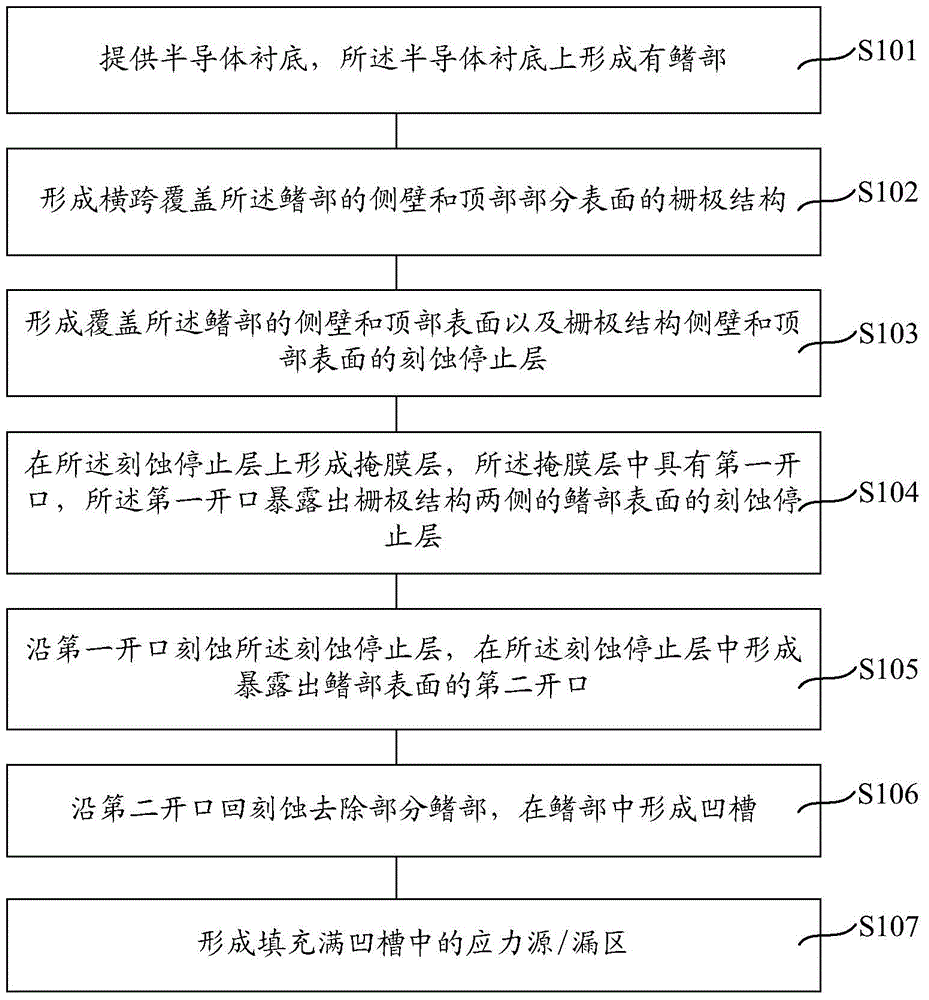
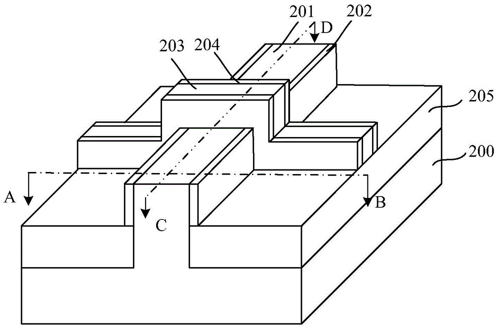
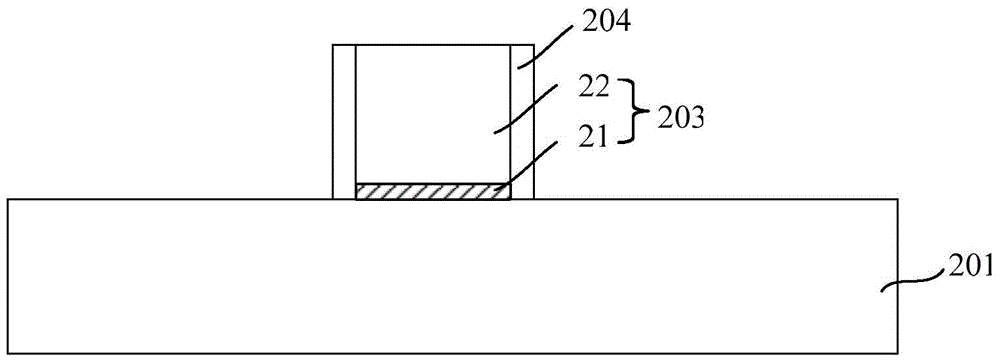
[0035] To study the formation process of fin field effect transistors, refer to figure 1 , Including the steps: step S101, providing a semiconductor substrate with a fin formed on the semiconductor substrate; step S102, forming a gate structure that spans the sidewall and top surface of the fin; step S103, forming Cover the sidewall and top surface of the fin and the etch stop layer on the sidewall and top surface of the gate structure; step S104, a mask layer is formed on the etch stop layer, the mask layer has a first An opening, the first opening exposes the etch stop layer on the surface of the fin on both sides of the gate structure; step S105, the etch stop layer is etched along the first opening, an...


PUM


Abstract

A method for forming a fin field effect transistor comprises the following steps: providing a semiconductor substrate, wherein fins are formed on the semiconductor substrate; forming gate structures which are across and cover part of the surfaces of the side walls and tops of the fins respectively; forming etch stop layers covering the fins and the gate structures respectively; forming a mask layer on each etch stop layer, wherein the mask layer is provided with a first opening which exposes the surface of the corresponding etch stop layer on the surface of the corresponding fin at the two sides of the corresponding gate structure; etching each etch stop layer along the first opening, and forming a second opening in each etch stop layer, wherein impurity elements entering in the etching process is left in the fins exposed by the bottoms of the second openings; performing first impurity element removal on the fins exposed by the bottoms of the second openings to remove the impurity elements left in the fins exposed by the second openings; performing back-etching along the second openings to remove part of the fins, and forming a groove in each fin; and forming stress source/drain regions filling the grooves. By using the method, the performance of the formed stress source/drain regions is improved.

Description

Technical field [0001] The invention relates to the field of semiconductor manufacturing, in particular to a method for forming a fin field effect transistor. Background technique [0002] The MOS transistor generates a switching signal by applying a voltage to the gate and adjusting the current through the channel region. However, when semiconductor technology enters the node below 45 nanometers, the traditional planar MOS transistor's ability to control the channel current becomes weak, causing serious leakage current. A fin field effect transistor (FinFET) is an emerging multi-gate device. It generally includes a semiconductor fin with a high aspect ratio, a gate structure covering part of the top and sidewalls of the fin, and a gate structure located on the gate. The source and drain regions in the fins on both sides of the structure, the gate structure of the fin-type field effect transistor can control the fins from the top and both sides, and has much stronger gate-to-cha...

Claims


Application Information

Patent Timeline
IPC IPC(8): H01L21/336
Inventor 张海洋郑喆
Owner SEMICON MFG INT (SHANGHAI) CORP
Why Eureka
Try Eureka