Double-active layer Cu2O/SnOp channel thin film transistor and preparation method thereof

A thin-film transistor, double-layer thin-film technology, applied in transistors, semiconductor/solid-state device manufacturing, semiconductor devices, etc., can solve the problems of large surface leakage current, low hole mobility, and high hole concentration, and improve the switching current ratio. , the preparation temperature is low, the effect of improving the mobility

Inactive Publication Date: 2016-03-30
SOUTH CHINA UNIV OF TECH
View PDF3 Cites 4 Cited by
  • Summary
  • Abstract
  • Description
  • Claims
  • Application Information

AI Technical Summary

Problems solved by technology

Currently, based on Cu 2 Some progress has been made in the research of p-channel TFT devices made of metal oxides such as O and SnO. However, such devices generally have problems such as low hole mobility, large surface leakage current, large off-state current, and high hole concentration.

Method used


Image

  • Double-active layer Cu2O/SnOp channel thin film transistor and preparation method thereof
  • Double-active layer Cu2O/SnOp channel thin film transistor and preparation method thereof
  • Double-active layer Cu2O/SnOp channel thin film transistor and preparation method thereof

Examples


Embodiment

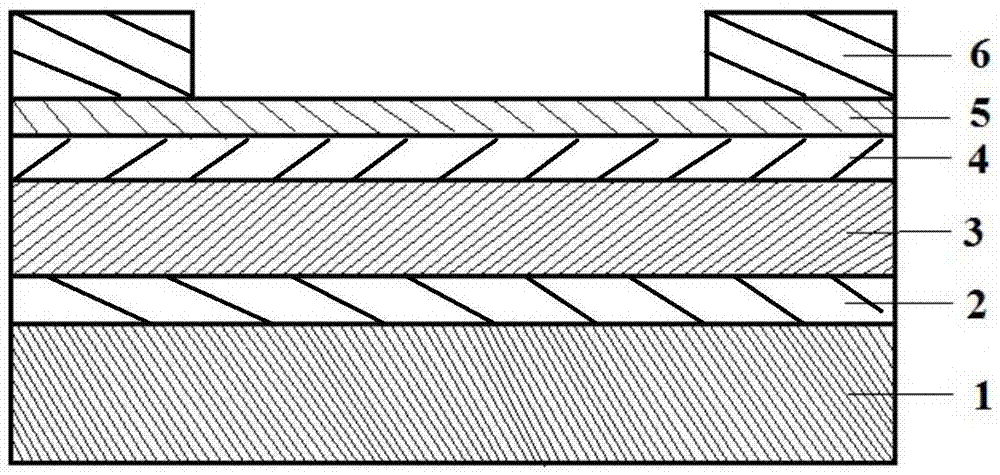
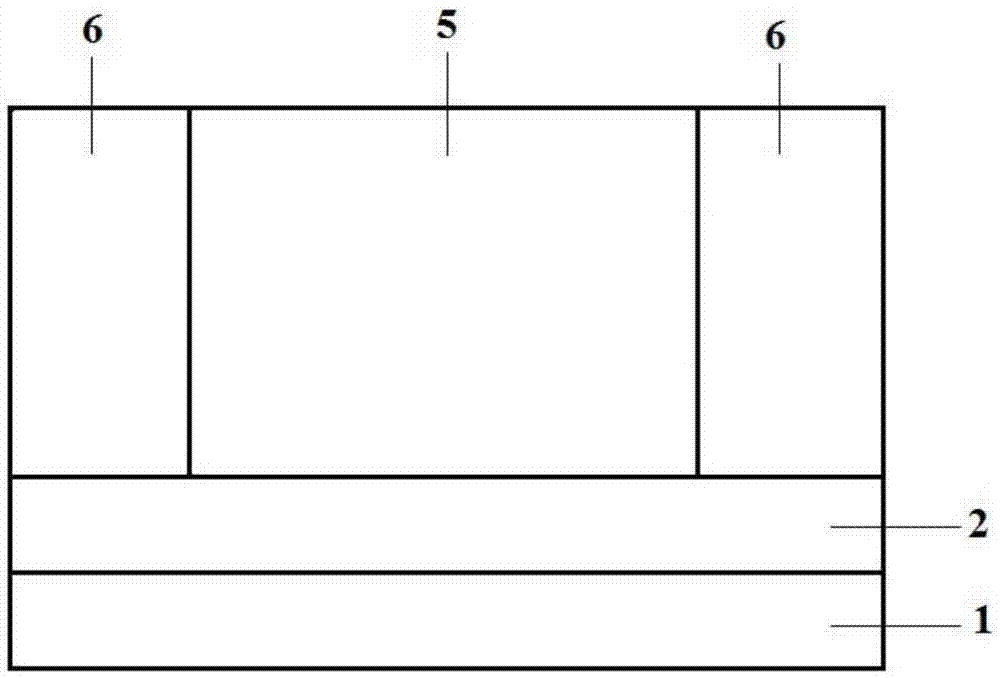
[0035] Cu of the double active layer structure of the present embodiment 2 The O / SnOp channel thin film transistor includes a substrate (1), a gate (2), a gate insulating dielectric layer (3), a p-type SnO semiconductor active layer (4), Cu 2 O semiconductor active layer (5), source electrode and drain electrode (6); its structural schematic diagram is as shown in Figure 1.

[0036] The gate partially covers the substrate, the gate insulating dielectric layer partially covers the gate, the p-type SnO semiconductor active layer completely covers the gate insulating dielectric layer, and the Cu 2 The O semiconductor active layer completely covers the p-type SnO semiconductor active layer.

[0037] The source and drain are relatively parallel.

[0038] The embodiment of the present invention also proposes the above-mentioned Cu 2 A method for preparing an O / SnOp channel thin film transistor, comprising:

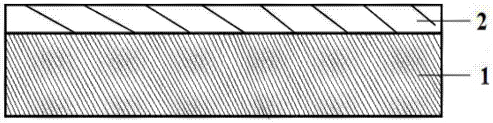
[0039] 1, make substrate: the substrate of the present embodiment is pl...


PUM


Abstract

The invention belongs to the technical field of semiconductors, and discloses a double-active layer Cu2O / SnOp channel thin film transistor and a preparation method thereof. The thin film transistor comprises a substrate, a grid electrode, a grid insulating medium layer, a first semiconductor active layer, a second semiconductor active layer, a source electrode and a drain electrode from bottom to top, wherein the first semiconductor active layer is a p-type SnO semiconductor active layer and the second semiconductor active layer is a Cu2O semiconductor active layer. According to the p-type SnO semiconductor active layer, oxygen vacancy is imported to properly optimize the valence band structure, so that the hole migration rate is improved; and through depositing a layer of Cu2O membrane on the SnO active layer, the surface leakage current is decreased, the switch current ratio is improved, the influences on the SnO layer from the external oxygen and water are decreased and the device stability is improved.

Description

technical field [0001] The invention relates to the field of semiconductor technology, in particular to a dual active layer structure Cu 2 O / SnOp channel thin film transistor and its preparation method. Background technique [0002] In recent years, flat panel display technology represented by active matrix liquid crystal display (AM-LCD) and active matrix organic light emitting diode display (AMOLED) has been rapidly developed. Thin-film transistor (TFT), as a key device for active flat-panel display drive, plays an important role in the display effect of flat-panel displays. Thin-film transistors mainly include silicon-based TFTs, organic TFTs and oxide TFTs, among which amorphous silicon thin-film transistors (a-SiTFT) and polysilicon thin-film transistors (p-SiTFT) are widely used in flat panel displays due to their relatively mature technology and good stability. , is still the mainstream TFT technology. [0003] In recent years, TFTs based on metal oxide semiconduct...

Claims


Application Information

Patent Timeline
Patent Type & Authority Applications(China)
IPC IPC(8): H01L29/786H01L21/336
CPCH01L29/78681H01L29/66742
Inventor 赵高位刘玉荣廖荣
Owner SOUTH CHINA UNIV OF TECH
Why Eureka
Try Eureka