
A kind of preparation method of cztsse thin film solar cell absorption layer

A thin-film solar cell and absorption layer technology, applied in circuits, photovoltaic power generation, electrical components, etc., can solve the problems of increased film surface roughness, poor film electrical properties, difficult film composition, etc., to improve crystal quality and reduce pores. , the effect of improving interface performance

Active Publication Date: 2018-07-10
CHINA ELECTRONIC TECH GRP CORP NO 18 RES INST
View PDF5 Cites 0 Cited by
  • Summary
  • Abstract
  • Description
  • Claims
  • Application Information

AI Technical Summary

Problems solved by technology

This will not only make the composition of the film difficult to control, but also the loss of the Sn-containing compound will lead to the formation of a large number of pores on the surface of the film, which will increase the surface roughness of the film, increase the number of grain boundaries, form more defects near the surface, and deteriorate the electrical properties of the film.

Method used


Image

  • A kind of preparation method of cztsse thin film solar cell absorption layer
  • A kind of preparation method of cztsse thin film solar cell absorption layer
  • A kind of preparation method of cztsse thin film solar cell absorption layer

Examples


Embodiment 1

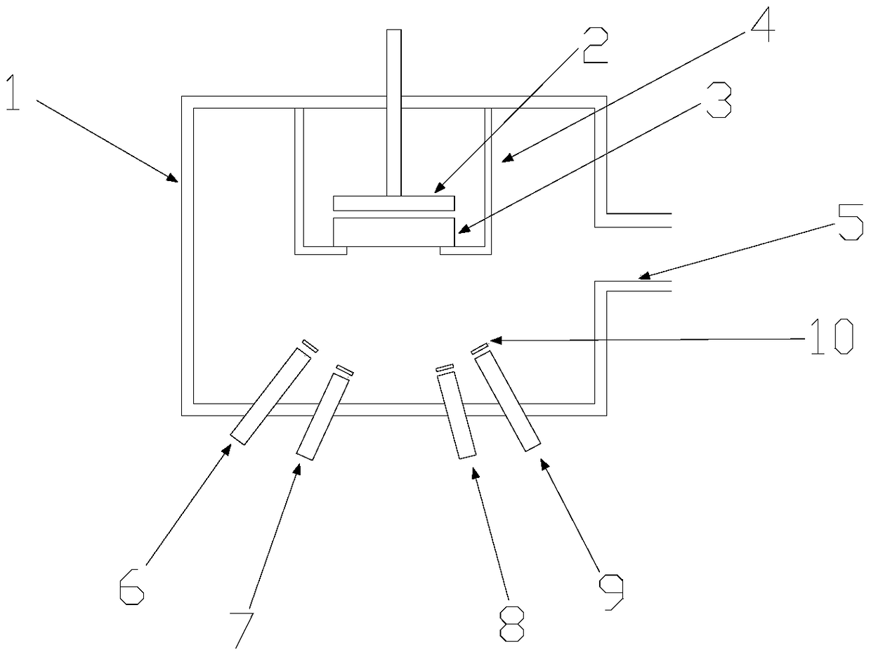
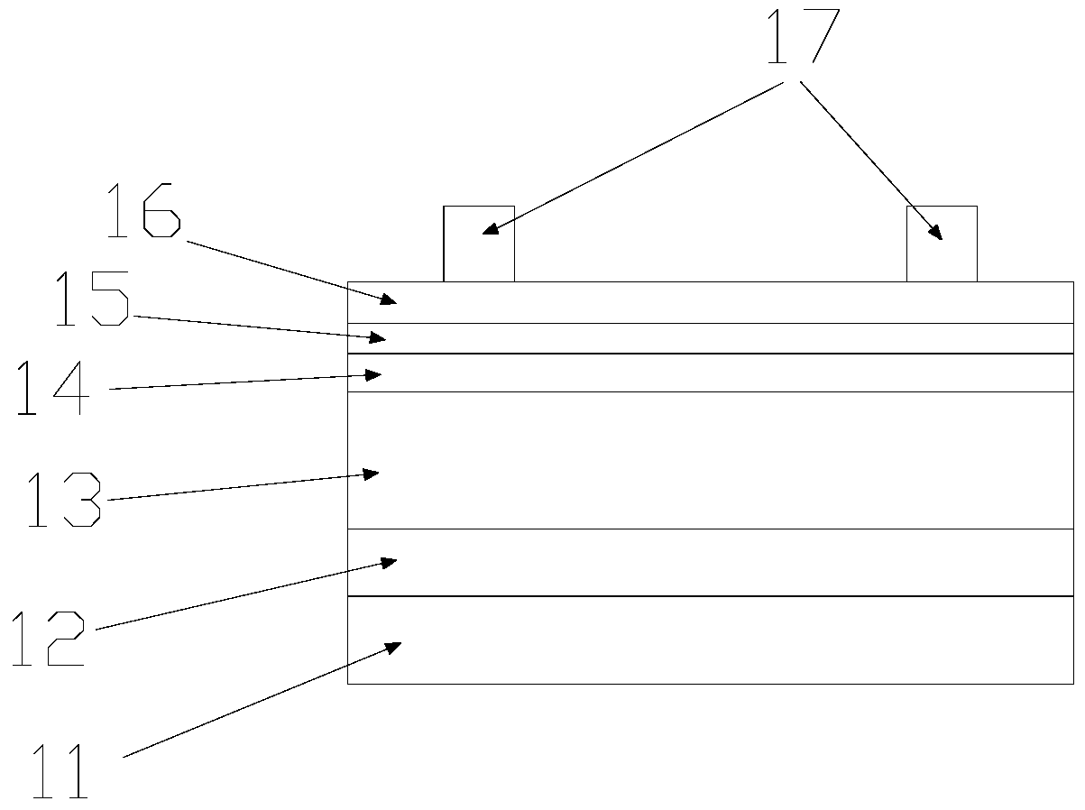
[0028] Embodiment 1, adopting soda-lime glass as the substrate 11, depositing a 1 μm thick Mo back electrode 12 on the substrate 11 by magnetron sputtering; preparing a CZTSSe absorbing layer 13 on the Mo back electrode; the CZTSSe absorbing layer The preparation process of 13 is: (1) placing the Mo-plated substrate in the sample holder 4 of the evaporation chamber 1, the sample holder is rotatable; a substrate heating device 2 is placed above the substrate 11; Cu evaporation source 6, The ZnS evaporation source 7, the Sn evaporation source 8, and the Se evaporation source 9 are evenly distributed under the evaporation chamber. The inside of the evaporation chamber 1 is equipped with a thermocouple for monitoring the evaporation temperature. The substrate and the Cu evaporation source 6, the ZnS evaporation source 7, An evaporation source baffle 10 is placed between the Sn evaporation source 8 and the Se evaporation source 9; (2) The evaporation chamber is evacuated to 3×10 by ...

Embodiment 2

[0031] A stainless steel foil with a thickness of 40 μm was used as the substrate, and other conditions were the same as in Example 1 to prepare a CZTSSe thin film solar cell with a stainless steel substrate structure.

Embodiment 3

[0033] A titanium foil with a thickness of 40 μm was used as the substrate, and other conditions were the same as in Example 1 to prepare a CZTSSe thin film solar cell with a titanium substrate structure.


PUM


Abstract

The invention discloses a preparation method for an absorption layer of a CZTSSe thin-film solar cell. The preparation method is implemented by two steps by using materials of Cu, ZnS, Sn, and Se as raw evaporation materials. At the first step, materials of Cu, Sn, and Se are evaporated to generate a Cu2SnSe3 ternay phase unit that is easy to generate and is not easy to decompose, wherein after generation of the Cu2SnSe3 ternay phase unit, formation and re evaporation of a Sn-contained compound can be effectively suppressed and thus generation of surface pores is reduced. At the second step, raw materials of ZnS, Sn, and Se are evaporated until the proportion of all element components reaches a near stoichiometric ratio requirement needed for preparing the absorption layer of the CZTSSe solar cell, and chemical combination of the materials of ZnS and the Cu2SnSe3 is carried out to generate a CZTSSe phase with a custerite structure. Because a Zn-contained compound deposited on a substrate is in a liquid phase structure and the formed hole can be filled with the Zn-contained compound easily, all elements can be induced to carry out combination reactions in holes to effectively reduce the holes, thereby improving the crystal quality of the thin film surface.

Description

technical field [0001] The invention belongs to the technical field of thin film solar cells, in particular to a method for preparing an absorbing layer of a CZTSSe thin film solar cell. Background technique [0002] The progress of human society is inseparable from the demand for energy. The development of industrialization has made non-renewable energy sources such as coal, oil, and natural gas frequently run out. At the same time, environmental pollution caused by the combustion of fossil energy has increasingly become a major threat to human survival. Therefore, it has become a common goal of all countries in the world to seek highly efficient and environmentally friendly renewable energy. Renewable energy mainly includes solar energy, nuclear energy, wind energy, water energy, etc. Among them, solar energy has the advantages of no noise, no pollution, inexhaustible, and not restricted by geographical conditions. It is the fastest growing and most dynamic energy in recen...

Claims


Application Information

Patent Timeline
Patent Type & Authority Patents(China)
IPC IPC(8): H01L21/02H01L31/032H01L31/18
CPCH01L21/02425H01L21/02568H01L21/02631H01L31/0326H01L31/18Y02E10/50Y02P70/50
Inventor 杨亦桐王赫张超邓朝文杨立徐睿赵彦民乔在祥
Owner CHINA ELECTRONIC TECH GRP CORP NO 18 RES INST
Learn More