Check patentability & draft patents in minutes with Patsnap Eureka AI!

Flash memory device

A flash memory device and storage unit technology, applied in the direction of electric solid-state devices, semiconductor devices, electrical components, etc., can solve problems such as floating body effect, affecting device programming speed and programming efficiency, etc., achieve stable programming efficiency, eliminate floating body effect, The effect of low programming voltage

Inactive Publication Date: 2016-04-06
SHANGHAI HUALI MICROELECTRONICS CORP
View PDF5 Cites 1 Cited by
  • Summary
  • Abstract
  • Description
  • Claims
  • Application Information

AI Technical Summary

Problems solved by technology

[0008] In view of the above existing problems, the present invention discloses a flash memory device to overcome the structure of the prior art flash memory device, only a small part of electrons can be injected into the floating gate as hot electrons, and most of the electrons flow out through the drain terminal, thereby affecting The programming speed and programming efficiency of the device are problematic, and the use of SOI flash memory devices is prone to the problem of floating body effect

Method used


Image

  • Flash memory device

Examples


Embodiment Construction

[0028] The present invention will be further described below in conjunction with the accompanying drawings and specific embodiments, but not as a limitation of the present invention.

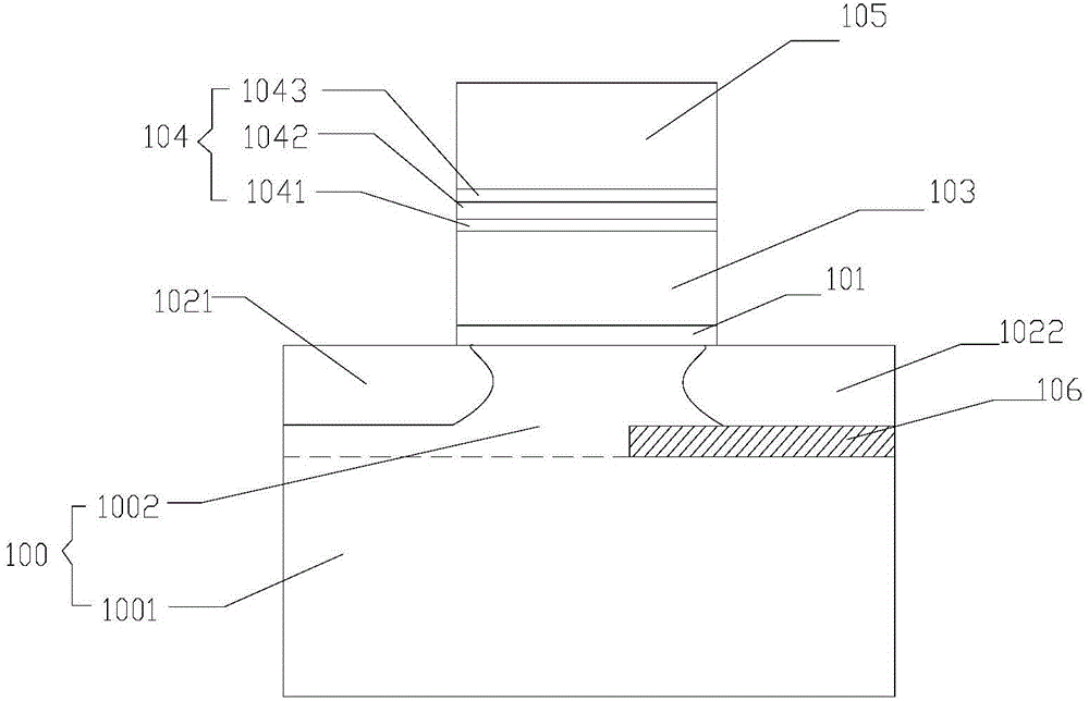
[0029] figure 1 is a schematic structural diagram of a flash memory device in an embodiment of the present invention; figure 1 Shown:

[0030] This embodiment relates to a flash memory device, the flash memory device includes a memory cell array area, the memory cell array area includes a first substrate 1001 and a second substrate 1002 disposed on the first substrate 1001, located on the above-mentioned first substrate 1001 Several memory cells are arranged on the second substrate 1002, the memory cell includes a floating gate (FloatingGate) 103 and a control gate 105 at the top of the floating gate 103, and the floating gate 103 and the control gate 105 pass through an ONO dielectric layer (including the first Oxide layer 1041, silicon nitride layer 1042 and second oxide layer 1043) 104 are ...


PUM


Abstract

The invention discloses a flash memory device. Through only arranging a buried oxide layer below a drain end, the modulation function of a two-dimensional electric field is utilized so that an electric field next to the drain end is improved and electron hole collision probability is improved, thereby improving hot carrier generation probability, changing more electrons to hot electrons for being injected into a floating gate, and greatly improving device programming efficiency. Furthermore holes which are generated by impact ionization can be discharged through a silicon substrate next to the buried oxide layer, thereby preventing hole accumulation, thoroughly eliminating a floating body effect and realizing stable device programming efficiency. Furthermore because the flash memory device greatly improves the device programming efficiency, the programming voltage of the device can be reduced. The relatively low programming voltage reduces dynamic power consumption of a circuit. Furthermore an influence by a drain-end interference can be reduced.

Description

technical field [0001] The invention relates to the technical field of semiconductor manufacturing, in particular to a flash memory device. Background technique [0002] Flash memory (Flashmemory) is a new type of non-volatile semiconductor memory developed based on EPROM and EEPROM. It has the characteristics of cheap price, relatively simple process, and can be easily and quickly erased and written many times. It has been widely used, mainly in portable devices and embedded systems. [0003] Norflash relies on hot electron injection to store data, that is, electrons are accelerated in the channel by the transverse electric field at the drain and source, and hot electrons are formed near the drain. Through phonon scattering, under the action of the vertical electric field of the gate, some electrons It will be injected into the floating gate through the tunnel oxide layer, and the threshold voltage of the device will change accordingly, so as to achieve the purpose of stor...

Claims


Application Information

Patent Timeline
IPC IPC(8): H01L27/115H01L29/788H01L29/06
Inventor 齐瑞生田志陈广龙
Owner SHANGHAI HUALI MICROELECTRONICS CORP
Features
  • R&D
  • Intellectual Property
  • Life Sciences
  • Materials
  • Tech Scout
  • Unparalleled Data Quality
  • Higher Quality Content
  • 60% Fewer Hallucinations
Learn More