Supercharge Your Innovation With Domain-Expert AI Agents!

Vertical gallium nitride power switch device and manufacturing method therefor

A technology of power switching devices and gallium nitride, which is applied in semiconductor/solid-state device manufacturing, semiconductor devices, electrical components, etc., can solve the problems of increasing the lateral size of the device, current collapse, large gate-drain spacing, etc., to improve the utilization rate , the effect of reducing the size

Inactive Publication Date: 2016-04-06
BEIJING HUAJINCHUANGWEI ELECTRONICS CO LTD +1
View PDF5 Cites 8 Cited by
  • Summary
  • Abstract
  • Description
  • Claims
  • Application Information

AI Technical Summary

Problems solved by technology

However, since the lateral device will form a high electric field region on the material surface on the drain side, surface leakage or surface breakdown of the device will occur; at the same time, the virtual gate effect of the surface state under high field will lead to the occurrence of current collapse; and , in order to increase the breakdown voltage, a larger gate-to-drain spacing is usually required, which increases the lateral size of the device

Method used


Image

  • Vertical gallium nitride power switch device and manufacturing method therefor
  • Vertical gallium nitride power switch device and manufacturing method therefor
  • Vertical gallium nitride power switch device and manufacturing method therefor

Examples


Embodiment Construction

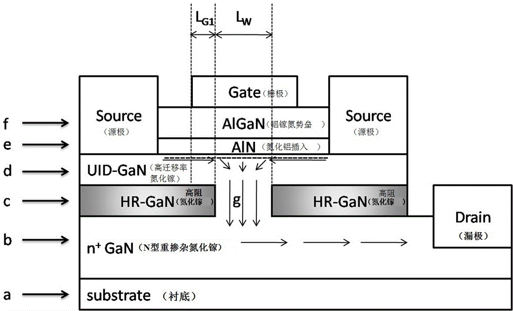
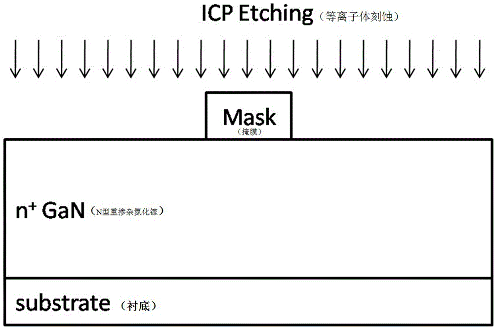
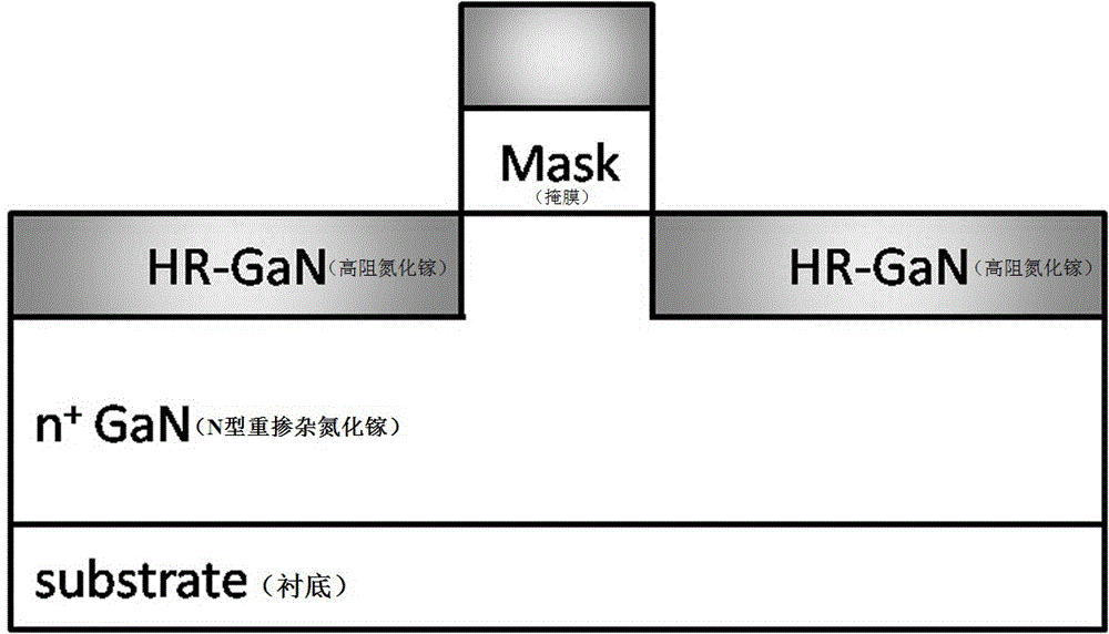
[0041] Hereinafter, the present invention will be described more fully with reference to the accompanying drawings, in which exemplary embodiments of the present invention are marked. This invention may, however, be embodied in many different forms and should not be construed as limited to the exemplary embodiments set forth herein. Rather, these embodiments are provided so that this disclosure will be thorough and complete, and will fully convey the scope of the invention to those skilled in the art.

[0042] For ease of description, spatially relative terms such as "upper," "lower," "left," and "right" may be used herein to describe the relationship of one element or feature relative to another element or feature shown in the figures. It will be understood that the spatial terms are intended to encompass different orientations of the device in use or operation in addition to the orientation depicted in the figures. For example, if the device in the figures is turned over, e...


PUM

PropertyMeasurementUnit
Thicknessaaaaaaaaaa
Thicknessaaaaaaaaaa
Resistivityaaaaaaaaaa

Abstract

The invention discloses a vertical gallium nitride power switch device and a manufacturing method therefor. The switch device comprises: a substrate (a); an N-type heavily-doped gallium nitride layer (b); a current window layer (c); an unintentionally-doped and high-migration-rate gallium nitride layer (d); an aluminum nitride insertion layer (e); an unintentionally-doped aluminum-gallium-nitrogen barrier layer (f); an ohmic contact source (Source); an ohmic contact drain (Drain); and a Schottky contact gate (Gate). According to the switch device, two high-resistance regions HR-GaN serve as current barrier regions, and a current window region g serves as a vertical current channel, so that a vertical gallium nitride based power device can be realized; and the drain and other electrodes (the gate and the drain) are located on different planes, so that the problems of current collapse and the like caused by surface electric leakage, surface breakdown and a virtual gate effect due to a high field region formed on the surface of a material can be avoided; and meanwhile, the size of the device can be reduced and the utilization rate of wafers can be increased.

Description

technical field [0001] The invention relates to the field of manufacturing electronic components, in particular to a vertical gallium nitride power switch device and a preparation method thereof. Background technique [0002] Gallium nitride material has the characteristics of large band gap, high saturation drift speed and high temperature resistance, and the heterostructure formed by it (such as AlGaN / GaN heterostructure) has high two-dimensional electron gas concentration and mobility, Therefore, it has obvious potential advantages in the production of high-performance power semiconductor devices, especially in the production of power electronic devices with high speed, low power consumption, and medium and low voltage. [0003] Since 2000, the research and development of GaN-based power semiconductor devices has made important progress. In 2000, UCSB reported a power electronic device with an AlGaN / GaN HEMT structure with a breakdown voltage of 570V; in 2008, UCSB rep...

Claims


Application Information

Patent Timeline
IPC IPC(8): H01L29/778H01L21/335
CPCH01L29/7788H01L29/66462H01L29/7786
Inventor 王晓亮肖红领李百泉王权冯春殷海波姜丽娟邱爱芹崔磊介芳
Owner BEIJING HUAJINCHUANGWEI ELECTRONICS CO LTD
Features
  • R&D
  • Intellectual Property
  • Life Sciences
  • Materials
  • Tech Scout
  • Unparalleled Data Quality
  • Higher Quality Content
  • 60% Fewer Hallucinations
Learn More