GaN-based LED structure and forming method thereof

A technology of LED structure and structure layer, applied in semiconductor devices, electrical components, circuits, etc., can solve the problem of insufficient internal quantum efficiency, and achieve the effect of improving compound luminous efficiency, reducing electron escape, and reducing hole barrier height.

Inactive Publication Date: 2016-04-06
BYD CO LTD
View PDF3 Cites 6 Cited by
  • Summary
  • Abstract
  • Description
  • Claims
  • Application Information

AI Technical Summary

Problems solved by technology

[0004] The present invention aims to solve one of the technical problems of insufficient internal quantum efficiency in the related art at least to a certain extent

Method used


Image

  • GaN-based LED structure and forming method thereof
  • GaN-based LED structure and forming method thereof
  • GaN-based LED structure and forming method thereof

Examples


Embodiment Construction

[0018] Embodiments of the present invention are described in detail below, examples of which are shown in the drawings, wherein the same or similar reference numerals designate the same or similar elements or elements having the same or similar functions throughout. The embodiments described below by referring to the figures are exemplary and are intended to explain the present invention and should not be construed as limiting the present invention.

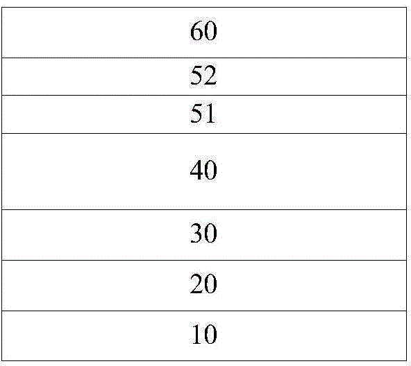
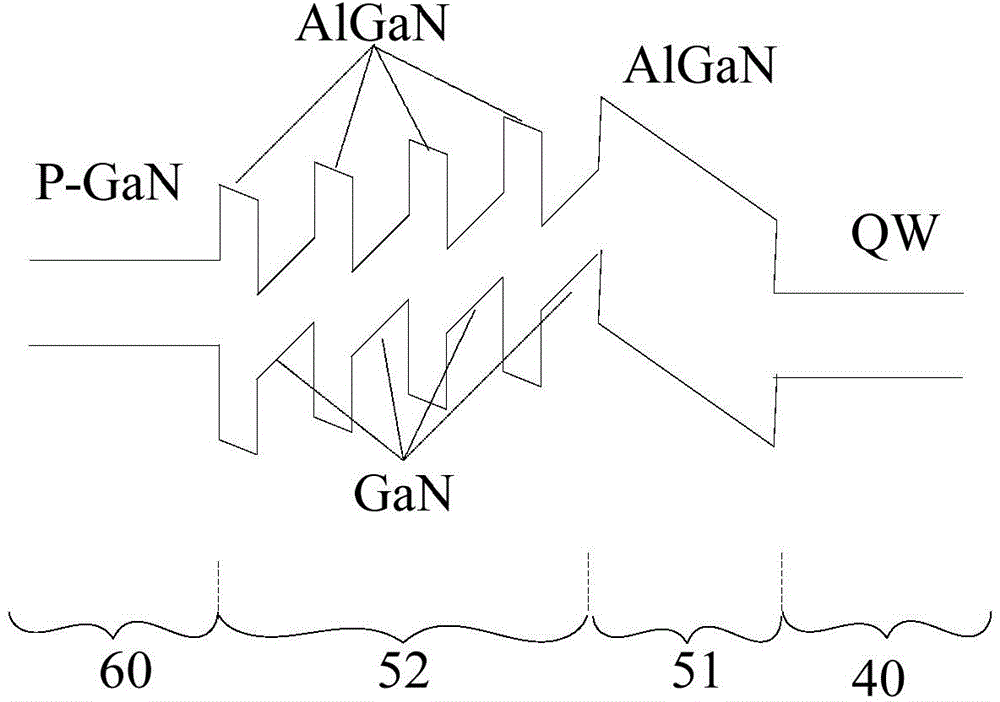
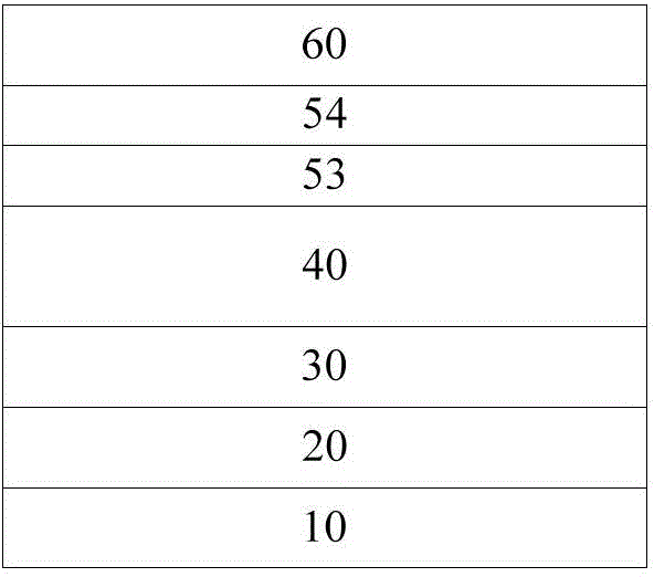
[0019] The first aspect of the present invention proposes a GaN-based LED structure, which may include: a substrate; a GaN layer of the first doping type located on the substrate; a quantum well light-emitting layer located on the GaN layer of the first doping type; a second doping type GaN layer on the quantum well light-emitting layer; an electron blocking layer; and a P electrode and an N electrode. It should be noted that the GaN layer of the first doping type may be an N-type GaN layer, and the GaN layer of the second doping...


PUM


Abstract

The invention discloses a GaN-based LED structure and a forming method thereof. The GaN-based LED structure provided by an embodiment of the invention comprises the components of a substrate; a first-doping-type GaN layer on the substrate; a quantum well light emitting layer on the first-doping-type GaN layer; a second-doping-type GaN layer on the quantum well light emitting layer; an electron barrier layer between the quantum well light emitting layer and a P-doping-type GaN layer, wherein the electron barrier layer comprises a block structure layer and a superlattice structure layer, the forbidden band width of the block structure layer is larger than that of the GaN, the superlattice structure layer is used for adjusting energy band inclination degree between the P-doping-type GaN layer and the block structure layer for reducing a hole potential barrier height; and a P electrode and an N electrode. According to the GaN-based LED structure, a composite structure in which the block structure layer and the superlattice structure layer are combined is utilized, thereby greatly improving composite light emitting efficiency of electron holes in the quantum well light emitting layer. Furthermore the GaN-based LED structure has advantages of simple structure, etc.

Description

technical field [0001] The invention belongs to the technical field of LED (Light Emitting Diode, light emitting diode), and specifically relates to a GaN-based LED structure and a forming method thereof. Background technique [0002] With the continuous development of the LED industry, LED has become a new generation of lighting source with its advantages of energy saving and environmental protection. At the same time, the performance of LED devices is also constantly developing in the direction of high brightness, low voltage and good reliability. In the existing technology, an electron blocking layer is inserted behind the quantum well light-emitting layer, so as to increase the spatial recombination probability of electron holes, improve internal quantum efficiency, and improve light efficiency. [0003] Common electron blocking layers include AlGaN block structure, AlGaN / GaN superlattice structure and other forms. The forbidden band width of AlGaN material is larger th...

Claims


Application Information

Patent Timeline
IPC IPC(8): H01L33/06H01L33/14H01L33/00
Inventor 吴明驰
Owner BYD CO LTD
Why Eureka
Try Eureka