Ultraviolet light-emitting diode with ultrathin aluminum-indium-nitrogen insertion layer and preparation method thereof
A technology of light-emitting diodes and insertion layers, which is applied to electrical components, circuits, semiconductor devices, etc., to achieve the effects of improving luminous efficiency, reducing energy band bending, and suppressing electron leakage
- Summary
- Abstract
- Description
- Claims
- Application Information
AI Technical Summary
Problems solved by technology
Method used
Image

Examples
no. 1 example
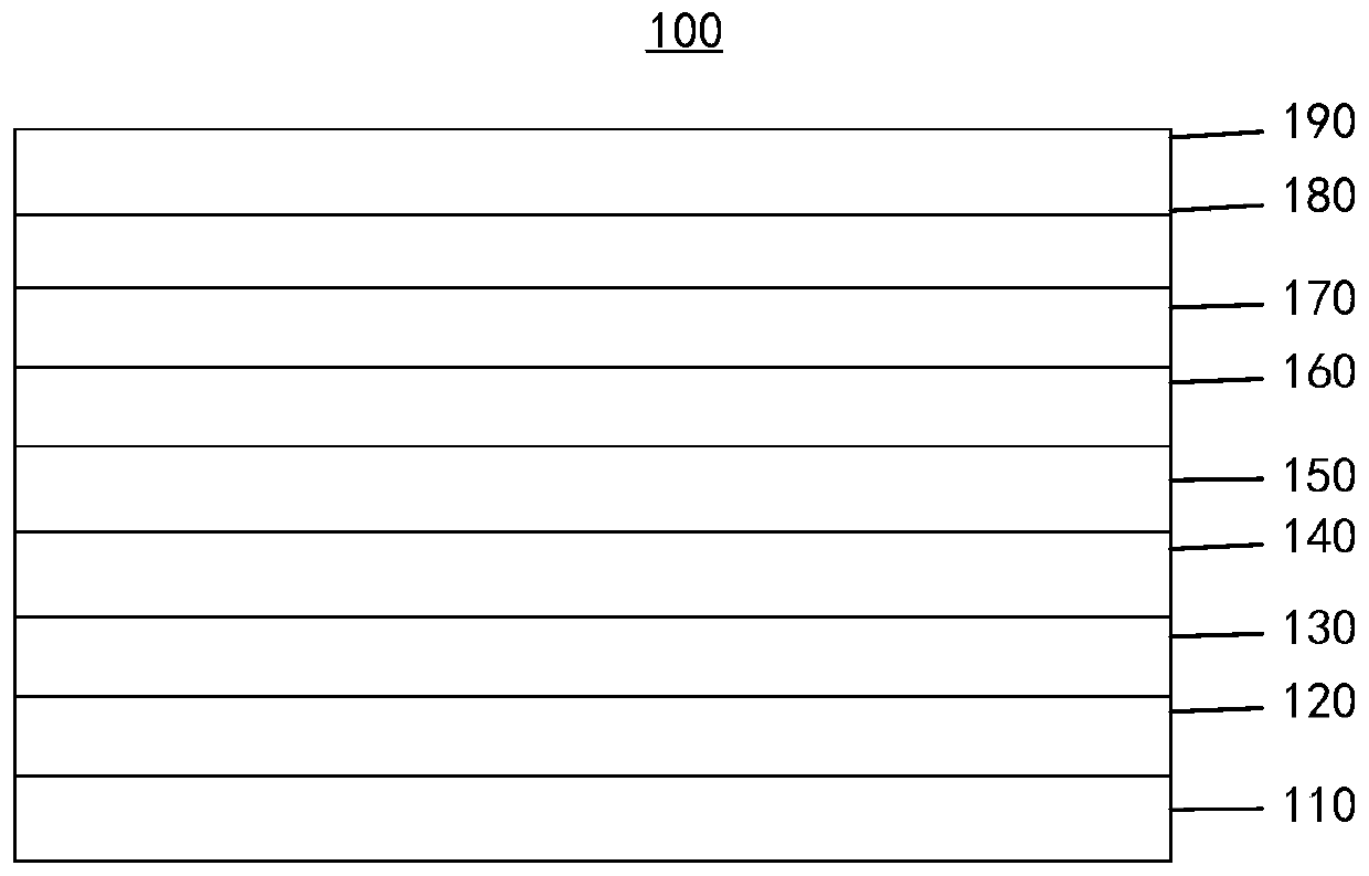
[0040] see figure 1 , the present embodiment provides an ultraviolet light-emitting diode 100 with an ultra-thin AlInN insertion layer, the ultraviolet light-emitting diode 100 includes a substrate 110 and a low-temperature buffer layer 120 and a high-temperature layer grown sequentially on the substrate 110 130 , n-type AlGaN layer 140 , light emitting active region 150 , insertion layer 160 , p-type AlGaN electron blocking layer 170 , p-type AlGaN layer 180 and contact layer 190 .
[0041]First, the substrate 110 can be made of sapphire; then, the low-temperature buffer layer 120 can be made of GaN or AlN, and the low-temperature buffer layer 120 can be epitaxially grown by magnetron sputtering or MOCVD; then, on the low-temperature buffer layer 120 The high-temperature layer 130 and the n-type AlGaN layer 140 are grown sequentially, wherein the thickness range of the n-type AlGaN layer 140 can be: 500nm-5000nm, and the silicon doping concentration is 1e17 / cm 3 ~1e20 / cm 3 ...
no. 2 example
[0049] This embodiment provides an ultraviolet light emitting diode 100, which is similar in structure to the first embodiment, except that the insertion layer 160 in this embodiment is doped with a small amount of Mg.
[0050] In the process of growing the insertion layer 160 on the last quantum barrier layer in the light-emitting active region 150, the insertion layer 160 with a wide bandgap is obtained by adjusting the Al flow rate and the In flow rate, and is doped with a small amount of Mg, and the Mg doping concentration Less than 1E19 / cm 3 , and the doping concentration of Mg increases gradually along the growth direction.
[0051] Doping the insertion layer 160 with a small amount of Mg can make the concentration of thermally activated holes higher, avoiding insufficient hole injection, thereby reducing the leakage of electrons from the light-emitting active region 150 to the p-type region, and further improving the quantum efficiency and luminous efficiency .
no. 3 example
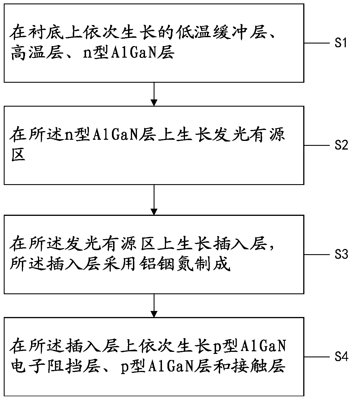
[0053] see figure 2 , this embodiment provides a method for manufacturing the ultraviolet light emitting diode 100, which is mainly used to prepare the ultraviolet light emitting diode 100 provided in the first embodiment or the second embodiment.
[0054] The preparation method of the ultraviolet light emitting diode 100 specifically includes the following steps:
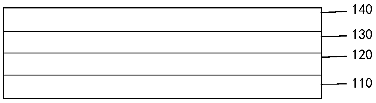
[0055] S1: see image 3 , a low-temperature buffer layer 120 , a high-temperature layer 130 , and an n-type AlGaN layer 140 are grown sequentially on a substrate 110 .
[0056] First, the substrate 110 can be made of sapphire; then, the low-temperature buffer layer 120 can be made of GaN or AlN, and the low-temperature buffer layer 120 can be epitaxially grown by magnetron sputtering or MOCVD; finally, on the low-temperature buffer layer 120 The high-temperature layer 130 and the n-type AlGaN layer 140 are grown sequentially, wherein the thickness range of the n-type AlGaN layer 140 can be: 500nm-5000nm, and the...
PUM
| Property | Measurement | Unit |
|---|---|---|
| Thickness | aaaaa | aaaaa |
| Growth temperature | aaaaa | aaaaa |
| Growth pressure | aaaaa | aaaaa |
Abstract
Description
Claims
Application Information
 - R&D
- Intellectual Property
- Life Sciences
- Materials
- Tech Scout
- Unparalleled Data Quality
- Higher Quality Content
- 60% Fewer Hallucinations
Browse by: Latest US Patents, China's latest patents, Technical Efficacy Thesaurus, Application Domain, Technology Topic, Popular Technical Reports.
© 2025 PatSnap. All rights reserved.Legal|Privacy policy|Modern Slavery Act Transparency Statement|Sitemap|About US| Contact US: help@patsnap.com