Sandwich packaging technique for preventing chip from deviating

A packaging process and chip technology, applied in the manufacture of electrical components, electrical solid devices, semiconductor/solid devices, etc., can solve the problems of position accumulation tolerance, heightening and thickening of the plastic package, chip displacement, etc., so that it is not easy to move and rotate, Prevent movement or rotation, good heat dissipation effect

Inactive Publication Date: 2016-04-13
JCET GROUP CO LTD
View PDF4 Cites 5 Cited by
  • Summary
  • Abstract
  • Description
  • Claims
  • Application Information

AI Technical Summary

Problems solved by technology

[0011] 2. The position of chip and solder paste cannot be grasped
[0012] In the method of dispensing solder paste for the rectifier diode, a traditional dispensing machine is used to apply solder paste to the bumps and platforms of the lower lead frame respectively, and this method of dispensing solder paste The biggest disadvantage of the design is the single spot coating, which can easily cause the positions of each spot to be different, and even cause serious position accumulation tolerances
If the solder paste applied is offset, due to the strong cohesive force of the solder paste, it will pull the chip on the solder paste, causing the chip to shift or rotate;
[0013] 3. The coplanarity of all metal pins cannot be mastered
[0014] If the amount of solder paste for each pin cannot be controlled, during reflow soldering, the solder paste will have strong cohesion during the process of cooling and solidification after the solder paste is heated and dissolved, and the upper , The lower lead frame is lifted up and down respectively, and because of the difference in the amount of solder paste, the size of the cohesion and shrinkage of the solder paste is different, resulting in that the outer pins of the lower lead frame and the outer pins of the upper lead frame are not on the same plane On the other hand, there is a gap between the metal pin and the surface of the mold, resulting in the quality problem of the overflow of the molding compound (see Figure 1b);
[0015] 4. The height of the plastic package must be increased and thickened
[0016] Because the amount of solder paste and position accuracy cannot be effectively controlled, the appearance size of the plastic package is forced to be wider and higher, resulting in cost waste and environmental pollution
[0017] If the above-mentioned diode chip is replaced with a triode or a multi-pole chip, since the tri-pole or multi-pole chip has two or more adjacent electrodes on the same surface, the chip moves slightly and the chip The alignment error of the rotating lead frame will often cause a short circuit between the chip electrodes
Therefore, the above process is not applicable to triode or multi-electrode chips.

Method used


Image

  • Sandwich packaging technique for preventing chip from deviating
  • Sandwich packaging technique for preventing chip from deviating
  • Sandwich packaging technique for preventing chip from deviating

Examples


Embodiment Construction

[0061] The present invention will be further described in detail below in conjunction with the accompanying drawings and embodiments.

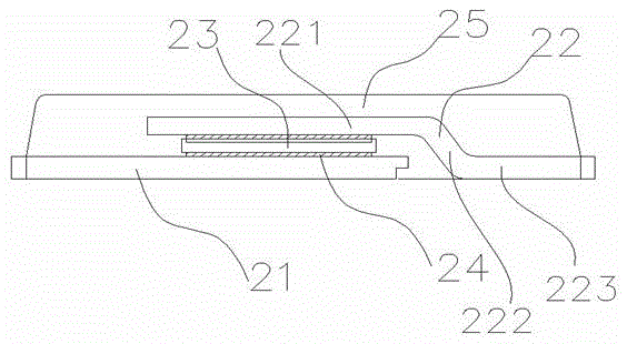
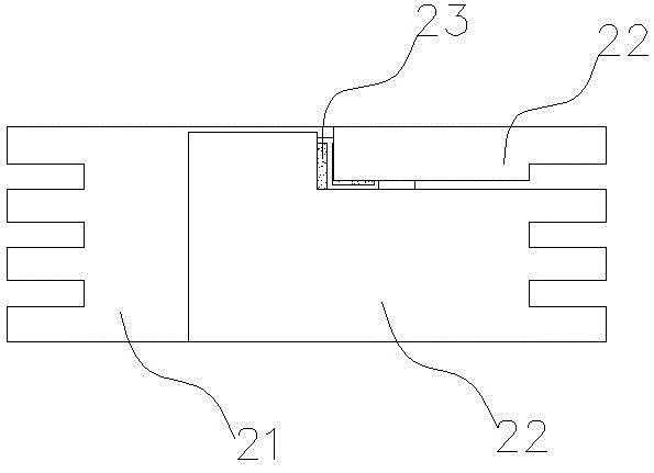
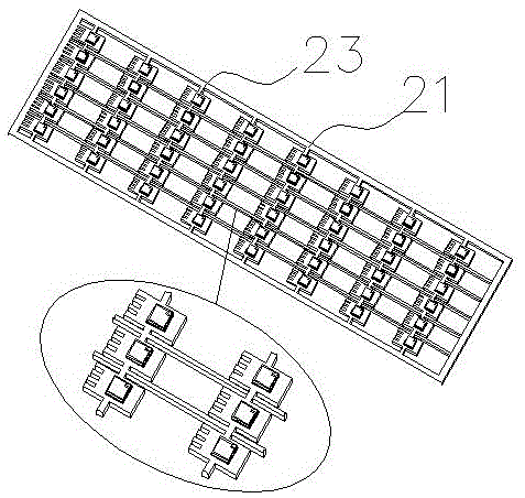
[0062] Such as Figure 8(a) ~ Figure 8(i) As shown, a sandwich packaging process method for preventing chip offset in this embodiment, the specific process steps are as follows:

[0063] Step 1, see Figure 8(a) , provide the first lead frame, the material of the first lead frame is alloy copper material, pure copper material, aluminum-plated copper material, zinc-plated copper material, nickel-iron alloy material, or other CTE range is 8*10^-6 / ℃~25*10^-6 / ℃ conductive material;

[0064] Step two, see Figure 8(b) , the base island area of ​​the first lead frame is coated with solder paste by screen printing, the purpose is to realize the bonding with the base island after the subsequent chip implantation, and the tin can be precisely controlled by adjusting the thickness of the screen plate and the area of ​​the opening The thickness, are...


PUM


Abstract

The invention relates to a sandwich packaging technique for preventing a chip from deviating. The sandwich packaging technique comprises the following steps: (1) providing a first lead frame; (2) coating an island region of the first lead frame with a solder paste; (3) implanting the chip into the first lead frame; (4) providing a second lead frame; (5) coating the second lead frame with the solder paste; (6) laminating the second lead frame on the chip on the upper surface of the first lead frame to form an overall frame; (7) pressing the upper surface and the lower surface of the overall frame formed in the step (6) with pressure plates and carrying out reflow soldering; (8) carrying out plastic packaging on the overall frame which is subjected to reflow soldering in the step (7); and (9) carrying out cutting or punching operation on a semi-finished product which is subjected to plastic packaging in the step (8), cutting or punching an original array-type plastic package body for separation, so as to prepare a sandwich package structure for preventing the chip from deviating. The sandwich packaging technique has the beneficial effect that the thickness, the area and the position of the solder paste can be easily controlled.

Description

technical field [0001] The invention relates to a sandwich packaging process method for preventing chip offset, and belongs to the technical field of semiconductor packaging. Background technique [0002] In recent years, with the continuous pursuit of power density in electronic products, whether it is Diode (secondary tube) or Transistor (transistor) packaging, especially the MOS products in Transistor are moving towards higher power, smaller size, faster , The trend of better heat dissipation is developing. There are more requirements for various electrical properties such as parasitic resistance, capacitance, and inductance in the packaging structure, the heat dissipation capability of the packaging structure, and the reliability of the packaging. The one-time manufacturing method of packaging is also gradually sprinting and challenging from single-chip packaging technology to high-density, high-difficulty and low-cost one-time packaging technology in small areas or eve...

Claims


Application Information

Patent Timeline
Patent Type & Authority Applications(China)
IPC IPC(8): H01L21/50H01L21/60H01L21/56
CPCH01L2224/32245H01L2224/97H01L2924/181H01L21/50H01L21/561H01L24/95H01L2021/60007
Inventor 梁志忠刘恺李政王孙艳
Owner JCET GROUP CO LTD
Why Eureka
Try Eureka