A p-type silicon solar cell and its preparation method

A technology of solar cells and p-type silicon, applied in the field of solar cells, can solve the problems of low conversion efficiency, achieve the effects of improving life, increasing open circuit voltage, and simplifying the process

Inactive Publication Date: 2018-01-12
HEBEI UNIVERSITY
View PDF5 Cites 0 Cited by
  • Summary
  • Abstract
  • Description
  • Claims
  • Application Information

AI Technical Summary

Problems solved by technology

[0004] One of the purposes of the present invention is to provide a p-type silicon solar cell to solve the problem of low conversion efficiency of existing p-type silicon solar cells

Method used


Image

  • A p-type silicon solar cell and its preparation method
  • A p-type silicon solar cell and its preparation method
  • A p-type silicon solar cell and its preparation method

Examples


Embodiment 1

[0029] Embodiment 1, a p-type silicon solar cell.

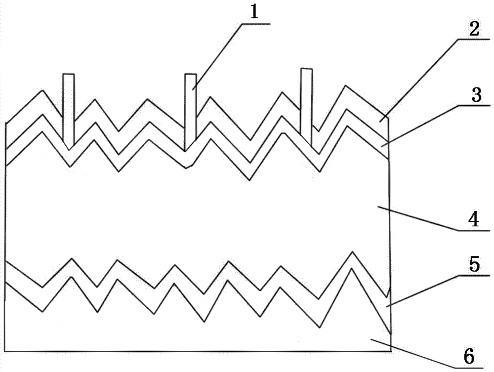
[0030] Such as figure 1As shown, the p-type silicon solar cell provided in this embodiment includes a p-type silicon substrate 4, and the p-type silicon substrate 4 may be a single crystal p-type silicon substrate or a polycrystalline p-type silicon substrate. On the front side of the p-type silicon substrate 4, n + doped layer 3, the n + An anti-reflection layer 2 is formed on the doped layer 3, and a front electrode 1 is formed on the anti-reflection layer 2 through screen printing and sintering processes. After sintering, the front electrode 1 will pass through the anti-reflection layer 2 and n + The doped layers 3 are in contact.

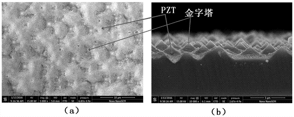
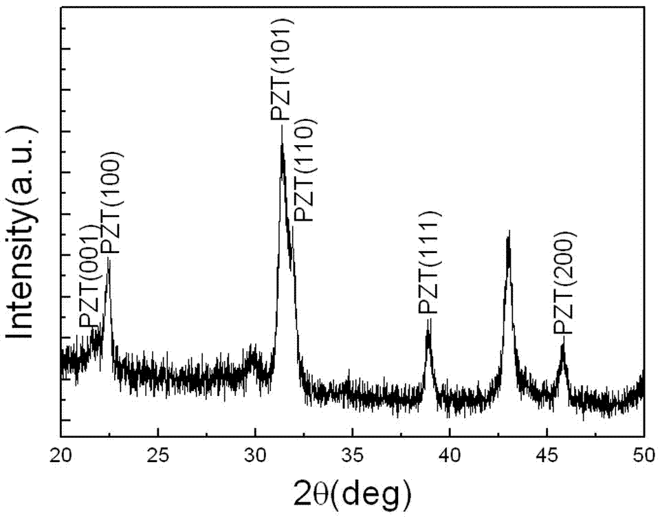
[0031] The back side passivation layer 5 is formed on the back side of the p-type silicon substrate 4, and the main material of the back side passivation layer 5 is a ferroelectric thin film material, and the ferroelectric thin film material can be, for example, lead zirconate titanate (PZT)...

Embodiment 2

[0032] Embodiment 2, a preparation method of a p-type silicon solar cell.

[0033] The preparation method of the p-type silicon solar cell provided in this embodiment includes the following steps:

[0034] ①. Select a p-type silicon substrate, and clean the selected p-type silicon substrate. After cleaning, texture the front and back of the p-type silicon substrate respectively. The p-type silicon substrate can be a single crystal p-type silicon substrate, or a polycrystalline p-type silicon substrate. When it is a single crystal p-type silicon substrate, alkali is generally used to texture it, and finally a regular pyramidal light trapping structure is formed. When it is a polycrystalline p-type silicon substrate, acid is generally used to texture it, and finally a regular uneven pit-shaped surface light-trapping structure is formed. In this embodiment, the p-type silicon substrate is a single crystal p-type silicon substrate, and the average height of the pyramids formed a...

Embodiment 3

[0055] Compared with embodiment 2, this embodiment adds a step after step ① and before step ②: planarizing the back side of the p-type silicon substrate. In this embodiment, the step of "planarizing the back of the p-type silicon substrate" is added, the purpose of which is to process the pyramid-shaped back into a slightly smooth back, that is, to smooth the top tip of the pyramid, so that the pyramid The apex-like structure of the structure and the sharp-edged horn-like structure at the bottom of the valley become smooth, and at the same time, the surface of the pyramid changes from rough to relatively smooth. After planarizing the back of the p-type silicon substrate, it should be ensured that a natural local contact can still be formed after the subsequent formation of the back passivation layer, which facilitates the subsequent preparation of the back electrode through printing and sintering processes.

[0056] In this embodiment, the back side of the p-type silicon subst...


PUM


Abstract

The invention provides a p-type silicon solar cell and a preparing method thereof. The p-type silicon solar cell comprises a p-type silicon substrate. The front surface of the p-type silicon solar cell is provided with an n<+> doped layer and a reflection reducing layer. Front anodes which penetrate the reflection reducing layer are manufactured. The front anodes are connected with the n<+> doped layer. The back surface of the p-type silicon substrate is provided with a back passivation layer. The back passivation layer comprises a film layer which is made of a ferroelectric film material or a doped ferroelectric film material. A back electrode is manufactured on the back passivation layer through a printing process and a sintering process. According to the p-type silicon solar cell, the ferroelectric film material is used as the main material of the back passivation layer of the cell, thereby greatly improving the open circuit voltage and shortcircuit current of the cell and improving conversion efficiency of the cell.

Description

technical field [0001] The invention relates to the technical field of solar cells, in particular to a p-type silicon solar cell and a preparation method thereof. Background technique [0002] The surface defects of crystalline silicon solar cells have a great influence on the performance of the cells. The open circuit voltage (V oc ), short circuit current (J sc ), fill factor (FF) and other main parameters largely depend on the level of surface defect density. The recombination loss of photogenerated carriers is one of the main ways of solar cell efficiency loss, and the surface recombination is the most important recombination loss. Reducing the surface defect density and reducing surface recombination are important means to improve the energy conversion efficiency of silicon solar cells. Passivation can effectively reduce the recombination of carriers, thereby improving the conversion efficiency of solar cells. Passivation usually has two methods: chemical passivatio...

Claims


Application Information

Patent Timeline
Patent Type & Authority Patents(China)
IPC IPC(8): H01L31/18H01L31/0216H01L31/068
CPCH01L31/02167H01L31/02168H01L31/068H01L31/1804H01L31/1868Y02E10/547Y02P70/50
Inventor 麦耀华陈兵兵陈剑辉许颖代秀红刘保亭
Owner HEBEI UNIVERSITY
Why Eureka
Try Eureka