SOI single-port SRAM (Static Random Access Memory) unit and a preparation method thereof

A manufacturing method and single-port technology, which is applied in the fields of electrical components, semiconductor/solid-state device manufacturing, static memory, etc., can solve the problems of large occupied area of ​​SOI single-port SRAM unit, weak anti-noise ability, poor stability, etc., to achieve convenient and comprehensive Customized SRAM chip, improved anti-noise ability, and suppressed floating body effect

Active Publication Date: 2016-05-04
SHANGHAI INST OF MICROSYSTEM & INFORMATION TECH CHINESE ACAD OF SCI
View PDF4 Cites 13 Cited by
  • Summary
  • Abstract
  • Description
  • Claims
  • Application Information

AI Technical Summary

Problems solved by technology

[0007] In view of the above-mentioned shortcoming of the prior art, the object of the present invention is to provide a kind of SOI single-port SRAM unit and manufacturing method thereof, be used to solve SOI single-port SRAM unit occupying a large area, poor stability, power leakage in the prior art The problem of high power consumption and weak anti-noise ability

Method used


Image

  • SOI single-port SRAM (Static Random Access Memory) unit and a preparation method thereof
  • SOI single-port SRAM (Static Random Access Memory) unit and a preparation method thereof
  • SOI single-port SRAM (Static Random Access Memory) unit and a preparation method thereof

Examples


Embodiment 1

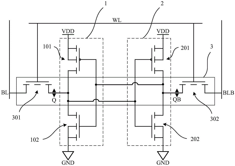
[0086] The present invention provides a SOI single-port SRAM unit, please refer to figure 1 , shown as a schematic diagram of the circuit principle of the SOI single-port SRAM cell, including:

[0087] The first inverter 1 is composed of a first PMOS transistor 101 and a first NMOS transistor 102;

[0088] The second inverter 2 is composed of a second PMOS transistor 201 and a second NMOS transistor 202;

[0089] The acquisition transistor 3 is composed of a third NMOS transistor 301 and a fourth NMOS transistor 302; the source of the third NMOS transistor 301 is connected to the output terminal of the first inverter and the input of the second inverter terminal, the gate is connected to the word line WL of the memory, and the drain is connected to the bit line BL of the memory; the source of the fourth NMOS transistor 302 is connected to the output end of the second inverter and the first inverter The gate is connected to the word line of the memory, and the drain is connec...

Embodiment 2

[0101] The present invention also provides a kind of manufacture method of SOI single-port SRAM unit, comprises the steps:

[0102] Step S1 is first performed: provide an SOI substrate including a back substrate, an insulating buried layer, and a top layer of silicon in sequence from bottom to top, and form a shallow trench isolation structure in the top layer of silicon to define an active region.

[0103] As an example, such as Figure 8 As shown, four active regions 20a, 20b, 20c, and 20d are defined. These four active regions are arranged in parallel in turn, and shallow trenches are formed around each active region, and the shallow trenches are filled with insulating materials to form shallow trenches. isolation structure. In this embodiment, the insulating material is silicon dioxide.

[0104] Then execute step S2: as Figure 9 As shown, an N well 30, a first P well 40 and a second P well 50 are fabricated in the top silicon according to the position of the active reg...


PUM


Abstract

The invention provides an SOI single-port SRAM unit and a preparation method thereof. The unit comprises a first phase inverter composed of a first PMOS transistor and a first NMOS transistor; a second phase inverter composed of a second PMOS transistor and a second NMOS transistor; an obtaining transistor composed of a third NMOS transistor and a fourth NMOS transistor. In the SRAM unit, the four transistors forming the first phase inverter and the second phase inverter are L-type gates; heavy dopant contact regions are arranged in the regions at the outer sides of the bending angles of the L-type gates. According to the unit and the method of the invention, leakage power consumption and transistor threshold voltage drift resulted from the floating body effect and parasitic triode effect in the PD SOI instrument can be effectively inhibited under the condition of sacrificing a relatively small unit area; the anti-noise capability of the unit is improved; the preparation technique of the invention introduces no extra mask plate and is fully compatible with the exiting logic technique; the inner part of the unit is a center symmetrical structure which is beneficial for matching the size and the threshold voltage of the MOS tube and for matching an array and is convenient for a full-custom SRAM chip.

Description

technical field [0001] The invention belongs to the field of memory design and production, and relates to an SOI single-port SRAM unit and a production method thereof. Background technique [0002] Since the invention of SOI technology in the 1980s, it has small parasitic capacitance, low power consumption, fast speed and natural anti-Single-Event-Latchup (SEL) ability compared with ordinary bulk silicon technology, making SOI The technology is very suitable for working in System-on-Chips (SoC), low power consumption and radiation resistance; in addition, Static Random Access Memory (SRAM) is widely used in consumer electronics, automotive electronics, processor level Cache and L2 cache; therefore, applying SOI technology to SRAM design has certain advantages. [0003] According to the degree of depletion of the MOS tube body region, SOI can be further divided into fully depleted (Full-Depleted, FD) SOI and partially depleted (Partially-Depleted, FD) SOI. For partially dep...

Claims


Application Information

Patent Timeline
Patent Type & Authority Applications(China)
IPC IPC(8): G11C11/41G11C11/412H01L21/8244H01L27/11
CPCG11C11/41G11C11/412H10B10/00H10B10/12
Inventor 陈静何伟伟伍青青罗杰馨王曦
Owner SHANGHAI INST OF MICROSYSTEM & INFORMATION TECH CHINESE ACAD OF SCI
Why Eureka
Try Eureka