Integrated circuit packaging structure and packaging technology based on Flip-chip connection

An integrated circuit and packaging process technology, applied in the field of integrated circuit packaging structure and packaging process, can solve the problems of high cost, unguaranteed packaging reliability, long production cycle, etc. short cycle effect

Inactive Publication Date: 2016-05-04
GUANGDONG CHIPPACKING TECH
View PDF3 Cites 2 Cited by
  • Summary
  • Abstract
  • Description
  • Claims
  • Application Information

AI Technical Summary

Problems solved by technology

Traditional integrated circuit flat no-lead packaging (QFN / DFN) mainly has the following shortcomings: first, the design and production cycle is long, and the cost is relatively high; second, the arrangement of bumps and the density of I / O are affected by the frame design and The frame manufacturing process is limited; the third is that after the frame is corroded and thinned, there is a risk of sliding in the mold, and the reliability of the package cannot be guaranteed; the fourth is that the thickness of traditional QFN / DFN products is still relatively large, which cannot meet the requirements of current portable devices. Demand for Small Volume, High Density Packaging

Method used


Image

  • Integrated circuit packaging structure and packaging technology based on Flip-chip connection
  • Integrated circuit packaging structure and packaging technology based on Flip-chip connection
  • Integrated circuit packaging structure and packaging technology based on Flip-chip connection

Examples


Embodiment Construction

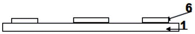
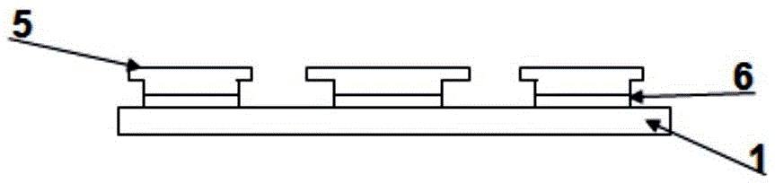
[0026] like Figure 9 As shown, a film-free and electroplating-free package based on Flip-chip connection, the package is mainly composed of metal bumps 2, chips 3, plastic package 4, chamfered silver-plated layer 5, and NiPdAu-plated layer 6 The chamfered silver-plated layer is a mutually independent silver-plated layer section, and metal bumps are planted on the chip, and the plastic package surrounds the metal bump, chip, NiPdAu-plated layer and chamfered silver-plated layer, and the metal Bumps, chips, chamfered silver-plated layers and NiPdAu-plated layers constitute the power and signal channels of the circuit.

[0027] The main process flow of a film-free and electroplating-free package based on Flip-chip connection: plating NiPdAu on the frame → growing a chamfered silver plating layer (through corrosion, the silver plating layer on the NiPdAu plating layer is formed as attached image 3 The chamfered groove shown) → wafer thinning → dicing → metal bumps on the chip →...


PUM


Abstract

The invention provides an integrated circuit packaging structure and a packaging technology based on Flip-chip connection. The integrated circuit packaging structure comprises a chip, metal projections arranged on the chip, nickel-plated palladium gold layers, chamfered silvered layers and a plastic-sealed body. The chamfered silvered layers are mutually-independent silvered segments. The chip is provided with the metal projections. The metal projections, the chip, the nickel-plated palladium gold layers and the chamfered silvered layers are plastically sealed in the plastic-sealed body. The metal projections, the chip, the chamfered silvered layers and the nickel-plated palladium gold layers form a power supply and signal channels of a circuit. The invention also provides the packaging technology of the above structure; the sliding risk of the integrated circuit packaging structure in a die is substantially lowered after a framework is thinned after corrosion; in addition, the pressure of a plastic-sealing material is reduced, and the integrated circuit packaging structure and the packaging technology are applicable to integrated circuit packaging.

Description

technical field [0001] The invention belongs to the technical field of integrated circuit packaging, and in particular relates to an integrated circuit packaging structure and packaging technology based on Flip-chip connections. Background technique [0002] Integrated circuit flat no-lead packaging (QFN / DFN), in recent years, with communication equipment (such as base stations, switches), smart phones, portable devices (such as tablet computers), wearable devices (such as smart watches, smart glasses, Smart bracelets, etc.) are popularized and developed rapidly, and are especially suitable for the packaging of large-scale integrated circuits with electrical requirements such as high frequency, high bandwidth, low noise, high thermal conductivity, small volume, and high speed. Integrated circuit flat no-lead packaging (QFN / DFN) effectively utilizes the packaging space of the lead pins, thereby greatly improving the packaging efficiency. Due to the short leads, small size of...

Claims


Application Information

Patent Timeline
Patent Type & Authority Applications(China)
IPC IPC(8): H01L21/48H01L21/60H01L23/495
CPCH01L2224/16245H01L2924/181H01L2924/00012H01L23/4952H01L21/48H01L24/10
Inventor 刘兴波梁大钟宋波
Owner GUANGDONG CHIPPACKING TECH
Why Eureka
Try Eureka