An in-situ test system for magnetoelectric stress coupling of nitride light-emitting diodes

A light-emitting diode, in-situ testing technology, applied in the direction of single semiconductor device testing, etc., can solve the problem of lack of real-time measurement and control

Active Publication Date: 2018-05-22
XIAMEN SANAN OPTOELECTRONICS TECH CO LTD
View PDF5 Cites 0 Cited by
  • Summary
  • Abstract
  • Description
  • Claims
  • Application Information

AI Technical Summary

Problems solved by technology

Due to the polarization field formed by the piezoelectric polarization of the III-nitride, the electric field changes when the current passes through the nitride, causing the polarization field to move, thereby changing the stress on the lattice, but there is currently no real-time Methods of Measurement and Control
[0003] In view of the fact that there is no in-situ method for testing the magnetoelectric stress change of nitride light-emitting diodes in the prior art, it is necessary to develop a new in-situ test system for magnetoelectric stress coupling of nitride light-emitting diodes

Method used


Image

  • An in-situ test system for magnetoelectric stress coupling of nitride light-emitting diodes
  • An in-situ test system for magnetoelectric stress coupling of nitride light-emitting diodes

Examples


Embodiment 1

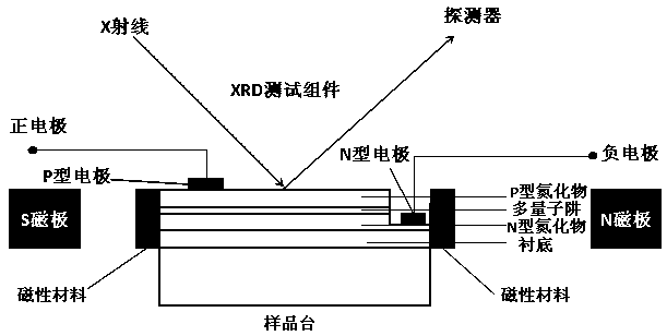
[0016] The structure of an in-situ test system for magnetoelectric stress coupling of nitride light-emitting diodes proposed in this embodiment is as follows: figure 1 shown. First, the nitride light-emitting diode includes a substrate, an N-type nitride, a multiple quantum well, a P-type nitride, a P-type electrode, and an N-type electrode. Electrode and negative electrode, through the current; secondly, the side wall is plated with a thickness of about 100nm Fe 3 o 4 The nitride light-emitting diodes of magnetic materials are placed on the sample stage of the XRD test components (including X-rays, detectors, etc.), and then the electromagnet magnetic field is set on both sides of the nitride light-emitting diodes as a magnetic field generating device, that is, when the nitride emits light A magnetic field of N / S magnetic poles is applied on both sides of the diode. Using the principle of X-ray diffraction, X-rays are irradiated on the nitride light-emitting diodes. The ω-2...

Embodiment 2

[0018] The difference from Embodiment 1 is that this embodiment changes the magnetic field by changing the magnetic pole of the magnetic field, transforming the original N magnetic pole into an S magnetic pole, and transforming the original S magnetic pole into an N magnetic pole to change the direction of the magnetic field. By changing the magnitude and direction of the magnetic field under a certain electric field condition, the obtained The direction and size of the electric field and magnetic field corresponding to the optimal stress and luminous efficiency of the nitride light-emitting diode can regulate the stress change of the nitride, thereby improving the luminous efficiency of the light-emitting diode, so that the nitride light-emitting diode can achieve the highest luminous efficiency output.


PUM


Abstract

The invention discloses an in-situ test system for magnetoelectric stress coupling of a nitride light emitting diode, comprising: a nitride light emitting diode, an external current source, an XRD test component and a magnetic field generating device, and is characterized in that the side wall of the nitride light emitting diode is formed Magnetic material, pass current through the P-type electrode and N-type electrode of the nitride light-emitting diode, place it on the sample stage of the XRD test assembly, generate a magnetic field around the nitride light-emitting diode through a magnetic field generating device, and make the nitride light-emitting diode Light-emitting diodes produce magnetic field-electric field-stress coupling effects, and use XRD single crystal diffraction to test the lattice constant of light-emitting diodes in the process of magnetic field and electric field changes in situ, and then control the magnitude of the magnetic field and electric field in situ, and adjust the stress change of nitrides , so that the light-emitting diode can obtain the highest luminous efficiency.

Description

technical field [0001] The invention relates to the field of semiconductor optoelectronic devices and testing, in particular to an in-situ testing system for magnetoelectric stress coupling of nitride light-emitting diodes. Background technique [0002] Nowadays, light-emitting diodes (LEDs), especially nitride light-emitting diodes, have been widely used in the field of general lighting due to their high luminous efficiency. However, since group III nitrides have a wurtzite structure, the atomic arrangement along the C-axis lacks an inversion symmetry center, forming group III atoms (Al / In / Ga) polar planes and N polar planes. The electronegativity of N atoms is greater than that of group III atoms, and the covalent bonds formed have strong ionic properties, resulting in spontaneous polarization. At the same time, when the crystal is subjected to external pressure, the positions of positive and negative ion cores change, resulting in piezoelectric polarization. Due to the ...

Claims


Application Information

Patent Timeline
Patent Type & Authority Patents(China)
IPC IPC(8): G01R31/26
Inventor 郑锦坚寻飞林邓和清杜伟华李志明伍明跃周启伦林峰李水清康俊勇
Owner XIAMEN SANAN OPTOELECTRONICS TECH CO LTD
Why Eureka
Try Eureka