Assembled hemisphere resonance micro gyroscope and processing process thereof

A hemispherical resonance, micro-gyroscope technology, applied in the field of micro-electromechanical and inertial navigation, can solve the problems of complex process of the hemispherical shell resonant gyroscope, affecting the working performance of the gyroscope, large supporting area, etc., and achieves low production cost, small size, The effect of simple processing technology

Active Publication Date: 2016-06-01
SOUTHEAST UNIV
5 Cites 6 Cited by

AI-Extracted Technical Summary

Problems solved by technology

[0004] The forming of the hemispherical resonator has been the bottleneck restricting its development so far. According to the information, so far, only the United States and Russia have produced relatively good finished products, and other countries are only in the research stage or the products produced have low performance.
Moreover, the process of making the hemispherical shell resonant gyroscope using the 3D-HARPSS process is c...

Method used

Step 1) in, can deposit nano getter in the circular cavity 7 of making, to guarantee the vacuum degree of vacuum encapsulation; The making of middle gyroscop...

Abstract

The invention discloses an assembled hemisphere resonance micro gyroscope, and belongs to the field of micro electronmechanical and inertia navigation. An upper layer glass substrate, a peripheral anchor point structure and a lower layer glass substrate are sequentially arranged from top to bottom; a round groove is formed in the center of the bottom surface of the upper layer glass substrate; the peripheral anchor point structure is of a hollow frame type structure; the round groove and a hollow region of the peripheral anchor point structure are communicated to form a cavity; a hemisphere casing harmonic oscillator is arranged in the center of the cavity; sixteen electrodes are arranged on the upper layer glass substrate at equal intervals; each electrode is connected with corresponding sixteen electrode holes; the electrode holes are formed in the upper layer glass substrate. The invention also discloses a processing process of the assembled hemisphere resonance micro gyroscope. The assembled hemisphere resonance micro gyroscope has the advantages that the encapsulation is realized; the production period is shortened; the production efficiency is improved. The processing process of the hemisphere casing harmonic oscillator and the uniform distribution type electrodes is simple; the dimension is small; the production cost is low; the production process is suitable for mass production.

Application Domain

Speed measurement using gyroscopic effectsGyroscopes/turn-sensitive devices

Technology Topic

PhysicsHarmonic oscillator +7

Image

  • Assembled hemisphere resonance micro gyroscope and processing process thereof
  • Assembled hemisphere resonance micro gyroscope and processing process thereof
  • Assembled hemisphere resonance micro gyroscope and processing process thereof

Examples

  • Experimental program(1)

Example Embodiment

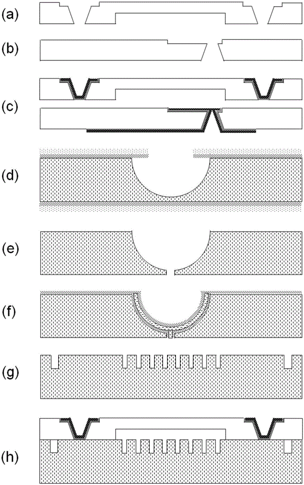
[0027] The technical solutions of the present invention will be described in detail below with reference to the drawings and specific embodiments, but the protection scope of the present invention is not limited to the embodiments.
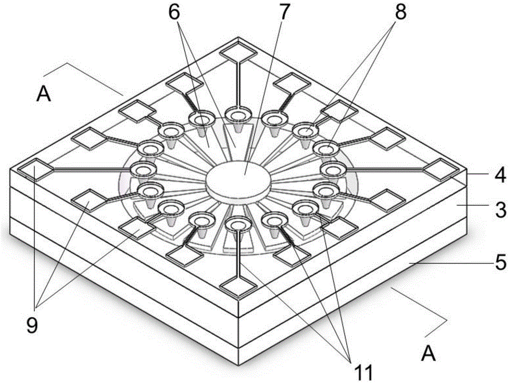
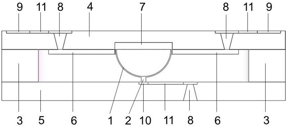
[0028] Such as Figure 1-2 As shown, an assembled hemispherical resonant micro gyroscope includes a hemispherical shell resonator 1, a supporting handle 2, a peripheral anchor structure 3, an upper glass substrate 4, a lower glass substrate 5, an electrode 6, and a circular groove 7. , The electrode hole 8, the pad 9, the metal electrode area 10 and the metal lead 11.
[0029] The upper glass substrate 4, the peripheral anchor point structure 3, and the lower glass substrate 5 are sequentially arranged from top to bottom. A circular groove 7 is provided in the center of the bottom surface of the upper glass substrate 4, and the peripheral anchor point structure 3 is hollow In the frame structure, the circular groove 7 and the hollow area of ​​the peripheral anchor point structure 3 are connected to form a cavity, and the hemispherical shell resonator 1 is arranged in the center of the cavity; the hemispherical shell resonator 1 is bonded to the center through the central support handle 2 5 on the lower glass substrate.
[0030] Electrodes 6 are arranged at equal intervals on the upper glass substrate 4, and each electrode 6 is respectively connected to the corresponding electrode hole 8. Among them, there are sixteen electrodes 6 and sixteen electrodes are provided in the upper glass substrate 4. Hole 8 is used to realize signal input and output; an electrode hole 8 corresponding to the hemispherical shell resonator 1 is provided on the lower glass substrate 5 to apply a reference voltage to the hemispherical shell resonator 1.
[0031] The hemispherical shell resonator 1, sixteen uniformly distributed electrodes 6 around the hemispherical shell resonator, and the peripheral anchor point structure 3 are processed on two silicon wafers.
[0032] There are pads 9 at equal intervals on the upper glass substrate 4, the pads 9 are square and sixteen, and the pads 9 are connected to the corresponding electrode holes 8 in the upper glass substrate 4 through metal leads 11; A metal electrode area 10 is provided on the lower glass substrate 5. The circular metal bonding area 10 is connected to the electrode hole 8 in the lower glass substrate 5 through a metal lead 11, and the electrode hole 8 is connected to the square metal on the bottom surface of the lower glass substrate 5. The pads are connected.
[0033] The diameter of the hemispherical shell resonator 1 is 1200~1500μm, and the thickness is 1~5μm.
[0034] The gap between the hemispherical shell resonator 1 and the electrode 6 is 5-20 μm; the overall size of the hemispherical shell gyroscope is 3000 μm×3000 μm×1200 μm.
[0035] Such as image 3 in, image 3 (A)- image 3 (K) Correspond to the following steps 1)-11). MEMS is a microelectronic mechanical system. LPCVD is low-pressure chemical weather deposition. HF etching is hydrofluoric acid etching.
[0036] A processing technology of an assembled hemispherical resonant micro gyroscope includes the following steps:
[0037] 1) Photoetch and wet etch on the reverse side of the upper PYREX7740 glass substrate to form a circular cavity, photoresist and wet etch on the front side to form electrode hole through holes, recoat the glue, photoetch and wet etch Etch to form square land slot and signal lead slot;
[0038] 2) Apply photoresist, photolithography, and wet etching on the front surface of the lower glass substrate to form a circular bonding area and lead groove, and apply photoresist, photolithography, exposure, development, and wet etching on the reverse side , Form electrode lead through holes;
[0039] 3) Photoresist, photolithography, exposure, development, sputtering metal chromium (Cr) and gold (Au) on the upper and lower glass substrates to form bonding areas, pads and signal leads;
[0040] 4) Clean the first silicon wafer and thermally grow SiO 2 , Apply photoresist, lithography and etch SiO 2 , Etch a circular opening in the center area, using SF 6 Plasma is etched isotropically to form hemispherical grooves;
[0041] 5) Apply photoresist, photolithography, exposure, and development on the back of the silicon wafer, and use the ICP process to etch the circular hole, so that the center hole penetrates the silicon wafer, so as to make the support handle;
[0042] 6) Thermally grown SiO 2 , LPCVD polysilicon, doping, annealing, removing the polysilicon on the surface, forming a hemispherical shell;
[0043] 7) Cleaning the second silicon wafer, thermally growing SiO on both sides 2 , Apply photoresist on the front side, lithography, exposure, develop, use ICP technology to etch the groove, and use CMP to thin the silicon wafer to the specified thickness;
[0044] 8) Perform silicon-glass anodic bonding between the second crystalline silicon wafer processed in step 7) and the upper glass substrate;
[0045] 9) LPCVD deposits SiO on the second crystalline silicon wafer 2 , Photolithography and etching using ICP technology until the deep groove at the bottom is etched to form electrodes and peripheral anchor point structures;
[0046] 10) The first silicon wafer processed through steps 4) to 6) is anodically bonded to the lower glass substrate with metal electrodes and leads, and HF is used to etch away the SiO 2 , Using same-sex etching gas SF6/XeF 2 Etch, remove photoresist;
[0047] 11) Use HF to etch SiO 2 , Release the structure, anodic bonding of the two structural layers, and vacuum packaging.
[0048] In step 1), a nano getter can be deposited in the circular cavity 7 made to ensure the vacuum degree of the vacuum package; the production of the middle gyroscope combines the MEMS bulk silicon processing technology, surface micromachining technology, and glass engraving Etching process and silicon-glass anode bonding process.

PUM

PropertyMeasurementUnit
Diameter1200.0 ~ 1500.0µm
Thickness1.0 ~ 5.0µm
tensileMPa
Particle sizePa
strength10

Description & Claims & Application Information

We can also present the details of the Description, Claims and Application information to help users get a comprehensive understanding of the technical details of the patent, such as background art, summary of invention, brief description of drawings, description of embodiments, and other original content. On the other hand, users can also determine the specific scope of protection of the technology through the list of claims; as well as understand the changes in the life cycle of the technology with the presentation of the patent timeline. Login to view more.

Similar technology patents

Method for casting and rolling aluminum alloy plate

InactiveCN102319735AReduce the time of hot rolling and cold rollingShorten the production cycleMetal rolling arrangementsScrapMetal
Owner:YONGJIE NEW MATERIAL CO LTD

Classification and recommendation of technical efficacy words

  • Improve production efficiency
  • Shorten the production cycle

Rapid investment casting method of complex thin-wall component

InactiveCN101862811AOmit the dewaxing processShorten the production cycleFoundry mouldsFoundry coresWaxInvestment casting
Owner:XUZHOU SHENGHAI MACHINERY MFG TECH
Why Eureka
Try Eureka