High-speed modulation light emitting diode and manufacturing method thereof

A technology for light-emitting diodes and a manufacturing method, which is applied to electrical components, circuits, semiconductor devices, etc., can solve the problems of low upper limit frequency of heterojunction bipolar transistors and cannot meet the needs of visible light communication, and achieves improved bandwidth, reduced diffusion capacitance, The effect of increasing the recombination rate

Active Publication Date: 2016-06-01
迪优未来科技(清远)有限公司
View PDF5 Cites 0 Cited by
  • Summary
  • Abstract
  • Description
  • Claims
  • Application Information

AI Technical Summary

Problems solved by technology

[0005] In order to solve the technical problem that the above-mentioned heterojunction bipolar transistor has a low upper limit frequency and cannot meet the needs of visible light communication, the present invention prov

Method used


Image

  • High-speed modulation light emitting diode and manufacturing method thereof
  • High-speed modulation light emitting diode and manufacturing method thereof
  • High-speed modulation light emitting diode and manufacturing method thereof

Examples


Embodiment Construction

[0036] The following will clearly and completely describe the technical solutions in the embodiments of the present invention with reference to the accompanying drawings in the embodiments of the present invention. Obviously, the described embodiments are only some, not all, embodiments of the present invention. Based on the embodiments of the present invention, all other embodiments obtained by persons of ordinary skill in the art without making creative efforts belong to the protection scope of the present invention.

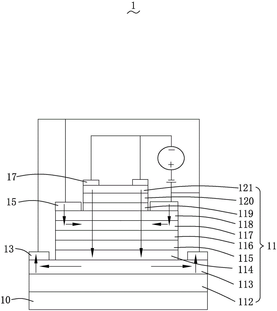
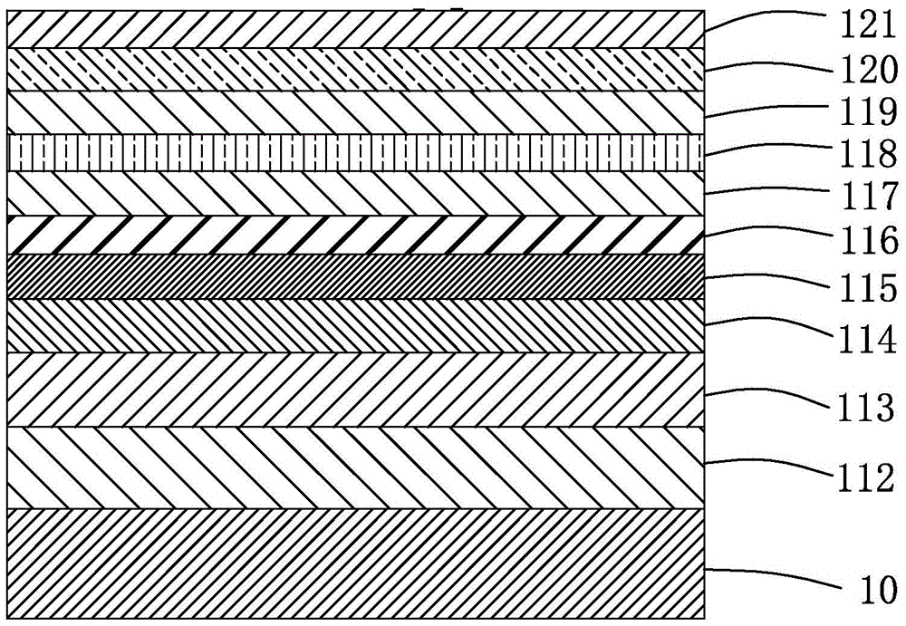
[0037] Please also refer to figure 1 and figure 2 , figure 1 It is a structural schematic diagram of the light-emitting diode chip provided by the present invention, figure 2 A schematic partial cross-sectional view of the substrate and the light-emitting epitaxial structure of the light-emitting diode chip provided by the present invention. The high-speed modulation light-emitting diode includes a light-emitting diode chip 1, and the light-emitting diode...


PUM


Abstract

The invention relates to a high-speed modulation light emitting diode and a manufacturing method thereof. The light emitting diode comprises a light emitting diode chip comprising a light emitting epitaxial structure. The light emitting epitaxial structure comprises a buffering layer, a first N-type gallium nitride contact layer, a gallium nitride depletion layer, a P-type aluminum gallium nitride electronic barrier layer, a first P-type indium gallium nitrogen layer, a quantum well layer, a second P-type indium gallium nitrogen layer, an N-type gallium nitride layer, a second N-type gallium nitride contact layer and a conductive layer. The quantum well layer is one of an undoped In<0.2>Ga<0.8>N/In<0.05>Ga<0.95>N quantum well layer and an indium gallium nitrogen/gallium nitride quantum well layer of a silicon doping barrier whose deposition quardi-period condensation is 5*1017 cm<-3>. The invention also provides a manufacturing method of the high-speed modulation light emitting diode. According to the invention, while the high-speed modulation light emitting diode is kept with light outputting power similar to that of a traditional light emitting diode, modulation width is increased.

Description

technical field [0001] The invention relates to the technical field of semiconductor manufacturing, in particular to a high-speed modulation light-emitting diode and a manufacturing method thereof. Background technique [0002] Semiconductor lighting, also known as solid-state lighting, refers to lighting using solid-state light-emitting devices as light sources, including light-emitting diodes (Light Emitting Diode, LED) and organic light-emitting diodes (Organic Light-Emitting Diode, OLED). In recent years, the semiconductor lighting technology known as "green lighting" has developed rapidly. Compared with traditional lighting sources, LED not only has low power consumption, long service life, small size, green environmental protection, but also has the advantages of good modulation performance and high response sensitivity. . Utilizing this feature of the LED, it can be used as lighting, and at the same time, the signal can be modulated onto the visible light beam of the...

Claims


Application Information

Patent Timeline
IPC IPC(8): H01L33/06H01L33/00
CPCH01L33/0075H01L33/06
Inventor 尹以安郭德霄范广涵
Owner 迪优未来科技(清远)有限公司
Why Eureka
Try Eureka