Interconnection structure of low-cost chip back through silicon via (TSV) and preparation method thereof

An interconnection structure and through-silicon via technology, applied in semiconductor/solid-state device manufacturing, semiconductor/solid-state device components, electrical components, etc., can solve the problem of high cost, achieve low cost, reduce process cost, and reduce difficulty.

Active Publication Date: 2016-06-08
HUATIAN TECH KUNSHAN ELECTRONICS
View PDF7 Cites 11 Cited by
  • Summary
  • Abstract
  • Description
  • Claims
  • Application Information

AI Technical Summary

Problems solved by technology

[0007] In order to solve the high cost of physical vapor deposition, electroplating, and rear wiring of Vialast TSVs, as well as the technical difficulties and reliability problems caused by pad connection and hole filling, the present invention proposes a low-cost chip The back through-silicon hole interconnection structure and its preparation method do not need chemical plating on the side wall of the through-silicon hole, and can avoid the use of deep-hole physical vapor deposition and deep-hole electroplating, and have the advantages of low cost, simple process and high reliability.

Method used


Image

  • Interconnection structure of low-cost chip back through silicon via (TSV) and preparation method thereof
  • Interconnection structure of low-cost chip back through silicon via (TSV) and preparation method thereof
  • Interconnection structure of low-cost chip back through silicon via (TSV) and preparation method thereof

Examples


Embodiment Construction

[0043] In order to make the present invention more comprehensible, the specific implementation manners of the present invention will be described in detail below in conjunction with the accompanying drawings. For convenience of description, the components in the structures in the drawings of the embodiments are not scaled according to the normal scale, so they do not represent the actual relative sizes of the structures in the embodiments.

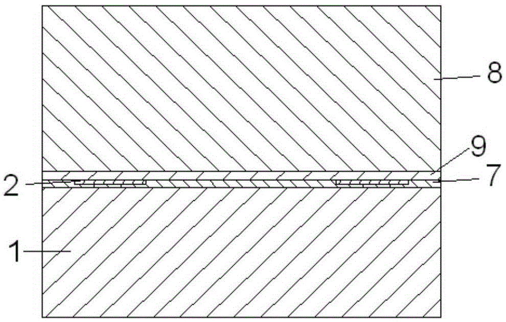
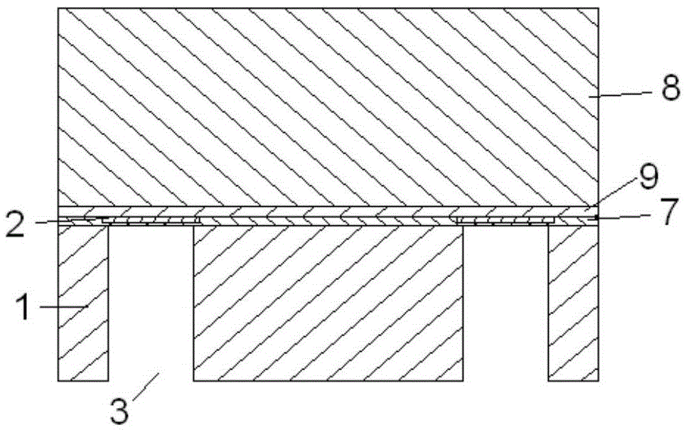
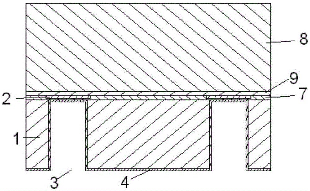
[0044] Such as Figure 7As shown, a low-cost chip back TSV interconnection structure includes at least one chip 1 with a bonding pad 2 on the front, and a through hole 3 corresponding to the bonding pad is formed on the back of the chip, and the through hole The bottom opening exposes the pad and the size is smaller than the size of the pad; the back of the chip and the sidewall of the through hole are covered with an insulating layer 4; the surface of the pad exposed by the bottom opening of the through hole is covered with A metal layer...


PUM


Abstract

The invention discloses an interconnection structure of a low-cost chip back through silicon via (TSV) and a preparation method thereof. The interconnection structure comprises at least one chip. The front surface of each chip is provided with a welding pad, and the back surface of the chip is provided with a through via corresponding to the welding pad. The bottom opening of the through via is exposed to the welding pad, and the size of the bottom opening of the through via is smaller than the size of the welding pad. The back surface of the chip and the sidewall of the through via are coated with an insulating layer. The surface of the welding pad, exposed out of the bottom opening of the through via, is formed with a metal layer of a certain thickness through the chemical plating process. The electrically conductive material is filled inside the through via through the non-metal plating process. According to the technical scheme of the invention, the electroless plating of the sidewall of the TSV is not required any more. Meanwhile, the deep hole physical vapor deposition and the deep hole plating are avoided, so that the interconnection structure is low in cost, simple in process and high in reliability.

Description

technical field [0001] The invention relates to the technical field of semiconductor packaging, in particular to a through-silicon hole interconnection structure on the back of a low-cost chip and a preparation method thereof. Background technique [0002] With the Internet of Things, the demand for miniaturization and multi-function of smart mobile terminals, three-dimensional integration, especially wafer-level packaging technology based on through-silicon vias (TSVs), plays an increasingly important role. [0003] Chinese patent 201520550505.5 proposes a TSV interconnect structure, including a silicon substrate and several TSVs. A semiconductor process layer is arranged on the silicon substrate. The TSVs penetrate the silicon substrate up and down, and are filled with metal to form metal pillars. , the metal post forms electrical communication with the semiconductor process layer, a passivation layer I is provided between the metal post and the inner wall of the TSV, and ...

Claims


Application Information

Patent Timeline
Patent Type & Authority Applications(China)
IPC IPC(8): H01L23/522H01L21/768
CPCH01L23/5226H01L21/76877H01L21/76898
Inventor 于大全邹益朝王晔晔肖智轶
Owner HUATIAN TECH KUNSHAN ELECTRONICS
Why Eureka
Try Eureka