Integrated protection mesa thyristor and manufacturing method thereof
A manufacturing method and technology of thyristors, which are applied in the direction of thyristors, semiconductor/solid-state device manufacturing, electrical components, etc., can solve problems such as increased leakage current, achieve the effects of improving reliability, improving charge distribution, and reducing leakage current
- Summary
- Abstract
- Description
- Claims
- Application Information
AI Technical Summary
Problems solved by technology
Method used
Image
Examples
Embodiment 1
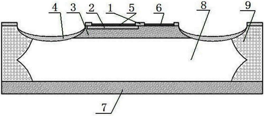
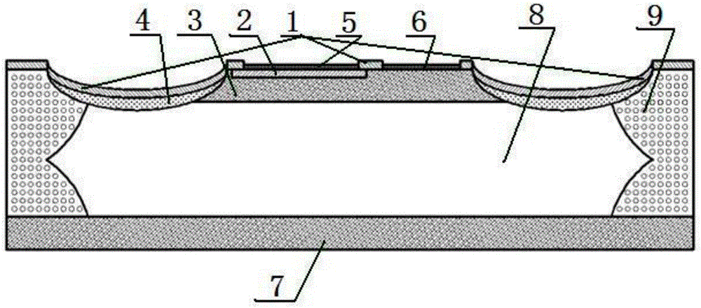
[0029] Embodiment 1: A kind of manufacture method of integrated protective mesa thyristor, it forms the PI glue passivation layer (1) of certain thickness on the glass passivation layer (4), this PI glue passivation layer (1) is in high-purity nitrogen Under protection, heat at 280-320° C. for 100-150 minutes to imidize the PI glue passivation layer (1) and fuse with the glass passivation layer (4) to form an integrated protective layer.
Embodiment 2
[0030] Embodiment 2: According to the manufacturing method of an integrated protective mesa thyristor described in Embodiment 1, the specific steps are:
[0031] 1. The oxide layer is formed by thermal growth of the chip, and the oxide layer is etched by photolithography for the first time, which is called punch-through lithography, and diffuses to form a punch-through region (9);
[0032] 2. On the basis of the punch-through region (9), use diffusion technology to diffuse the boron-based region on the front and back sides of the chip to form the base region (3) and anode (7);
[0033] 3. On the basis of the base area (3), use photolithography technology to carry out photoetching etching for the second time to the oxide layer, which is called opening the secondary cathode area to form the cathode area (2);
[0034] 4. Use photolithography technology to carry out the third photoetching etching on the oxide layer, which is called opening the mesa groove. Through the method of me...
Embodiment 3
[0040] Embodiment 3: According to the manufacturing method of an integrated protective mesa thyristor described in Embodiment 1, the specific steps are:
[0041] 1. The oxide layer is formed by thermal growth of the chip, and the oxide layer is etched by photolithography for the first time, which is called punch-through lithography, and diffuses to form a punch-through region (9);
[0042] 2. On the basis of the punch-through region (9), use diffusion technology to diffuse the boron-based region on the front and back sides of the chip to form the base region (3) and anode (7);
[0043] 3. On the basis of the base area (3), use photolithography technology to carry out photoetching etching for the second time to the oxide layer, which is called opening the secondary cathode area to form the cathode area (2);
[0044] 4. Use photolithography technology to carry out the third photoetching etching on the oxide layer, which is called opening a mesa groove. Through the method of mesa...
PUM
| Property | Measurement | Unit |
|---|---|---|
| Thickness | aaaaa | aaaaa |
Abstract
Description
Claims
Application Information

