A novel wafer thinning method

A new type of wafer technology, applied in electrical components, semiconductor/solid-state device manufacturing, circuits, etc., can solve problems such as affecting the test yield and difficult to clean small particles, to improve the quality of thinning and test yield, avoid The effect of secondary pollution

Active Publication Date: 2016-06-22
TIANSHUI HUATIAN TECH
View PDF7 Cites 12 Cited by
  • Summary
  • Abstract
  • Description
  • Claims
  • Application Information

AI Technical Summary

Problems solved by technology

During the process of filming on the wafer surface, the edge of the wafer cannot be tightly attached to the film, plus the individual bubbles formed by the film, the mixture of particles formed during wafer thinning and cooling water (sewage) along the film The gap between the edge of the wafer and the wafer penetrates to the surface of the wafer, and the sewage drills into the surface of the wafer, especially the small particles are difficult to clean, which not only affects the test yield, but also needs to be cleaned with a large amount of water

Method used


Image

  • A novel wafer thinning method
  • A novel wafer thinning method
  • A novel wafer thinning method

Examples


Embodiment 1

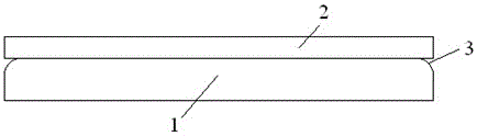
[0032] Take the polyimide solution, then take polytetrafluoroethylene according to 20% of the quality of the polyimide solution taken, add the polytetrafluoroethylene into the polyimide solution, put it on a rolling machine, roll, and stir evenly , to form a coating liquid; use a coating machine to coat the coating liquid on the front of the original wafer, so that the coating liquid evenly and tightly covers the front of the original wafer and the chamfering of the edge, and bake at a temperature of 60 ° C After 20 minutes, the coating solution is hardened to form a covering layer, which realizes seamless protection for the chips on the original wafer. Set the process parameters according to the existing coarse grinding process requirements on the thinning machine, and carry out rough grinding to the original wafer to achieve the rough grinding thickness of the original wafer required by the rough grinding process; press the existing rough grinding process on the thinning mach...

Embodiment 2

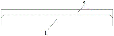
[0034]Take the PTFE UV adhesive film, cover the front surface of the original wafer and the edge chamfer with the PTFE UV adhesive film, bake at 50°C for 10 minutes, and the PTFE UV adhesive film will soften , to remove the air bubbles between the PTFE UV film and the original wafer, and the PTFE UV film is tightly pasted on the front of the wafer and the chamfering of the edge to form a covering layer, which is opposite to the original The chip on the wafer realizes seamless protection; on the thinning machine, the process parameters are set according to the existing rough grinding process requirements, and the original wafer is roughly ground to meet the coarse grinding process requirements. Thickness; on the thinning machine, the process parameters are set according to the existing fine grinding process requirements, and the original wafer after rough grinding is finely ground to achieve the thickness and roughness of the wafer after fine grinding required by the fine grindi...


PUM


Abstract

According to a novel wafer thinning method, polytetrafluoroethylene is added into a polyimide solution which is to be rolled and stirred uniformly to form coating liquid; the coating liquid is coated on the front surface of an original wafer to cover the surface of the original wafer and chamfers between the front surface of the original wafer and edges to form a cover layer; otherwise, a polytetrafluoroethylene coating or a UV coating is made to cover the front surface of the original wafer and subjected to low-temperature baking to enable a cover layer to form on the surface of the original wafer and the chamfers between the front surface of the original wafer and edges to form a cover layer; coarse grinding and fine grinding are carried out on the original wafer according to present technology; illumination is carried out to enable cracking of the cover layer; and plasma cleaning is carried out to remove the cracked cover layer so as to obtain the thinned wafer. The thinning method can prevent secondary pollution to the surface of the wafer in a thinning process; the wafer thinning quality and the test yield rate can be raised; cleaning by a lot of water is not needed; a lot of water resources are saved; and a good basis is provided for subsequent pressure welding technology.

Description

technical field [0001] The invention belongs to the technical field of semiconductor packaging for electronic device manufacturing, and relates to a wafer thinning method, in particular to a novel wafer thinning method. Background technique [0002] From the cross-sectional structure of integrated circuits, most integrated circuits are manufactured on the shallow surface layer of silicon base material. The integrated circuit manufacturing process puts forward high requirements on the dimensional accuracy, geometric accuracy, surface cleanliness and surface microlattice structure of the wafer. Therefore, in hundreds of processes, thinner wafers cannot be used, and only wafers of a certain thickness can be used to transfer and tape out during the process. Usually, before the integrated circuit is packaged, it is necessary to remove a certain thickness of base material from the backside of the wafer. This process is called wafer backside thinning process, and the correspondin...

Claims


Application Information

Patent Timeline
Patent Type & Authority Applications(China)
IPC IPC(8): H01L21/02
CPCH01L21/02013H01L21/02016H01L21/02118H01L21/0212H01L21/02282
Inventor 吕岱烈慕蔚邵荣昌
Owner TIANSHUI HUATIAN TECH
Why Eureka
Try Eureka