

TFT array substrate manufacture method
A manufacturing method and array substrate technology, applied in semiconductor/solid-state device manufacturing, electrical components, electrical solid-state devices, etc., can solve the problems of ITO residue, increase in TFT size, and unfavorable improvement of pixel density, so as to increase pixel density and reduce effect of size
- Summary
- Abstract
- Description
- Claims
- Application Information
AI Technical Summary
Problems solved by technology
Method used
Image

Examples
Embodiment Construction
[0051] In order to further illustrate the technical means adopted by the present invention and its effects, the following describes in detail in conjunction with preferred embodiments of the present invention and accompanying drawings.
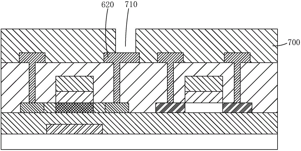
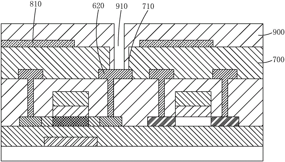
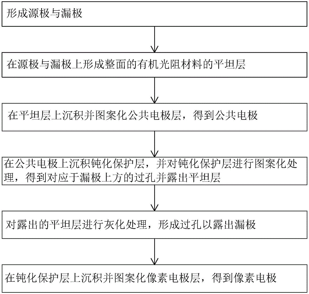
[0052] see Figure 3-14 , the following with FFS (FringeFieldSwitching, fringe field switching technology) type CMOS (ComplementaryMetalOxideSemiconductor, Complementary Metal Oxide Semiconductor) TFT array substrate making as a preferred embodiment of the present invention, the preparation method of the TFT array substrate provided by the present invention, specifically includes the following step:
[0053] Step 1, such as Figure 4 As shown, a base substrate 10 is provided, a first metal layer is deposited on the base substrate 10, and the first metal layer is patterned to obtain a light-shielding layer 20; The base substrate 10 forms a buffer layer 23 .
[0054] Specifically, the base substrate 10 is a transparent substrate, preferably a...
PUM
 Abstract
Description
Claims
Application Information