Trap state regulation and control based nonvolatile multi-bit micro/nanometer resistive random access memory and use method therefor

A resistive variable memory, non-volatile technology, applied in the direction of electrical components, etc., can solve difficult problems such as multi-bit storage performance, achieve good environmental compatibility, good compatibility, and realize the effect of efficient utilization

Inactive Publication Date: 2016-06-22
横峰县虹联铝业有限公司
View PDF5 Cites 4 Cited by
  • Summary
  • Abstract
  • Description
  • Claims
  • Application Information

AI Technical Summary

Problems solved by technology

[0003] Although researchers at home and abroad have obtained some achievements in non-volatile RRAM, in order to obtain non-volatile multi-bit storage performance, researchers will construct gate voltage or design special device structure when designing devices, and a few do not Resistive memory that needs to build a gate voltage or a special device structure has only two resistance states, and it is difficult to achieve multi-bit storage performance

Method used


Image

  • Trap state regulation and control based nonvolatile multi-bit micro/nanometer resistive random access memory and use method therefor
  • Trap state regulation and control based nonvolatile multi-bit micro/nanometer resistive random access memory and use method therefor
  • Trap state regulation and control based nonvolatile multi-bit micro/nanometer resistive random access memory and use method therefor

Examples


Embodiment 1

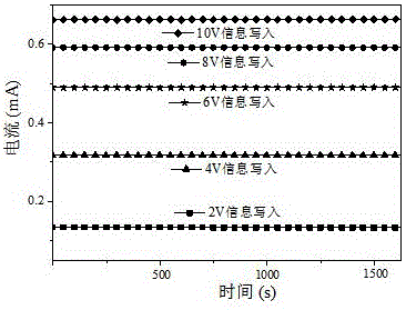
[0046] figure 2 After the micro / nano resistive memory of the present invention is written in 2V, 4V, 6V, 8V, 10V voltage, the memory performance test is performed. Adjust the function generator connected to the electrodes at both ends of the micro / nano resistive variable memory to a reading voltage of 0.5V, and then adjust the voltage to a writing voltage, and the writing voltage is 2V, 4V, 6V, 8V, 10V, after the voltage information is written, adjust back to the read voltage of 0.5V. Such as figure 2 As shown, after the voltages of 2V, 4V, 6V, 8V, and 10V are written, the micro / nano resistive memory has different resistance states. Sn-doped ZnO micro / nanowires have trap levels such as impurity levels, surface states, and intrinsic defects, and different write voltages can fill trap levels of different depths. When the trap is filled with electrons, the resistance state of the micro / nano resistive memory changes.

Embodiment 2

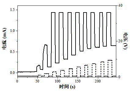
[0048] image 3 It is a diagram of the change of current with time after the voltage of 2V, 4V, 6V, 8V, and 10V is written in the micro / nano resistive memory of the present invention. Specifically, first adjust the function generator connected to the electrodes at both ends of the micro / nano resistive variable memory to a reading voltage of 0.5V, then adjust the writing voltage to 2V, 4V, 6V, 8V, and 10V respectively, and wait for the voltage information After writing, adjust back to the reading voltage of 0.5V and test the stability of the device current increasing with time. Such as image 3 As shown, after the voltages of 2V, 4V, 6V, 8V, and 10V are written, the holes in the traps are filled with electrons, the writing voltage is removed and the reading voltage is applied. The write voltage has a specific resistance state, and the resistance state can be maintained for a long time. When the holes in the trap are filled with electrons, the electrons are localized by the t...

Embodiment 3

[0050] Figure 4 to Figure 8 It is the repeatable reading and writing performance test of the micro / nano resistive memory of the present invention when the writing voltage is 2V, 4V, 6V, 8V, and 10V. Specifically: step 1, adjust the function generator connected to the electrodes at both ends of the micro / nano resistive variable memory to a reading voltage of 0.5V, and then adjust the voltage to 2V, 4V, 6V, 8V, and 10V for information writing input; Step 2, adjusting the voltage across the micro / nano resistive variable memory back to a voltage of 0.5V to read information; Step 3, placing the micro / nano resistive variable memory in a 70°C environment for signal erasing; Step 4, return to room temperature, and the resistance state of the micro / nano resistive variable memory returns to the initial state; repeat the cycle from step 1 to step 4 to detect the repeatability of the micro / nano resistive variable memory, except for the write voltage, all steps The reading voltage is a D...


PUM


Abstract

The invention discloses a trap state regulation and control based nonvolatile multi-bit micro/nanometer resistive random access memory and a use method therefor. The resistive random access memory comprises an insulating substrate, a single Sn-element-doped ZnO one-dimensional micro/nanowire, electrodes, a packaging material and the like; the single Sn-element-doped ZnO one-dimensional micro/nanowire is put on the insulating substrate, and electrodes are welded at the two ends of the nanowire respectively; and the single Sn-element-doped ZnO one-dimensional micro/nanowire and the electrodes are packaged on the insulating substrate by the packaging materials. In information write-in, a write-in voltage is applied between the electrodes at the two ends; in nonvolatile multi-bit storage, the write-in voltage is applied between the electrodes at the two ends, then the write-in voltage is removed and a read voltage is applied; in information erasure, the write-in voltage is applied between the electrodes at the two ends, then the write-in voltage is removed and the read voltage is applied; then the resistive random access memory is put in an environment at a temperature of 70 DEG C and then put in a room temperature. According to the resistive random access memory, response and storage to electric field information is realized; and meanwhile, the resistive random access memory is simple and convenient in process, small in volume, light and portable, high in compatibility and capable of realizing efficient utilization.

Description

technical field [0001] The present invention relates to the technical field of micro / nano materials, and relates to a non-volatile multi-bit micro / nano resistive memory that utilizes trap states to regulate resistance states. Large and small electrical signals are used to read, write, store and erase information. Background technique [0002] In recent years, among all kinds of new non-volatile memory devices, resistive memory has the advantages of simple structure, low energy consumption, fast response speed, good repeatability of reading and writing, long information storage time, non-destructive reading, and The advantages of extended assembly and CMOS process compatibility have attracted extensive attention from scientists at home and abroad. As a key physical phenomenon in RRAM, resistive switching effect is widely found in electrolyte materials, perovskite materials, and transparent metal oxides. The current-voltage characteristic curve of the resistive switching dev...

Claims


Application Information

Patent Timeline
Patent Type & Authority Applications(China)
IPC IPC(8): H01L45/00
CPCH10N70/00H10N70/801
Inventor 赵婕程抱昌
Owner 横峰县虹联铝业有限公司
Why Eureka
Try Eureka