Manufacturing method of ultra-thin printed circuit board and ultra-thin printed circuit board

A technology of printed circuit board and manufacturing method, which is applied in the field of circuit board manufacturing to achieve the effects of avoiding scrapping, avoiding deformation, and preventing the phenomenon of jamming

Active Publication Date: 2016-06-22
SHANGHAI MEADVILLE ELECTRONICS +1
View PDF9 Cites 9 Cited by
  • Summary
  • Abstract
  • Description
  • Claims
  • Application Information

AI Technical Summary

Problems solved by technology

This also brings new challenges to the manufacturing process of printed circuit boards

Method used


Image

  • Manufacturing method of ultra-thin printed circuit board and ultra-thin printed circuit board
  • Manufacturing method of ultra-thin printed circuit board and ultra-thin printed circuit board
  • Manufacturing method of ultra-thin printed circuit board and ultra-thin printed circuit board

Examples


Embodiment 1

[0072] The manufacture method of ultra-thin printed circuit board is characterized in that, comprises the steps:

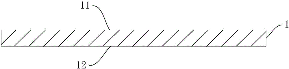
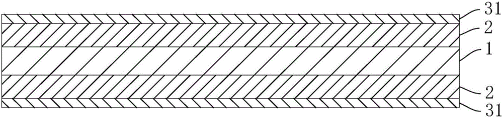
[0073] a. If figure 1 As shown, a carrier 1 is provided, and the carrier 1 is made of a polymer material. The carrier board 1 has a first surface 11 and a second surface 12 oppositely disposed. Such as figure 2 As shown, the metal layer 2 is respectively disposed on the first surface 11 and the second surface 12 of the carrier 1 . The metal layer is a copper layer, an aluminum layer or an alloy metal layer. The first copper foil 31 is provided on the metal layer 2 . The first copper foil 31 is bonded to the metal layer 2 .

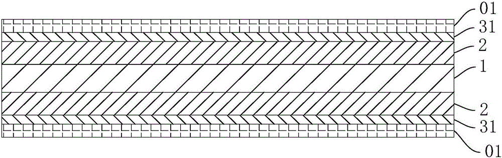
[0074] b. Perform electroplating treatment on the carrier plate 1 provided with the metal layer 2 and the first copper foil 31 . The specific process of electroplating treatment is as follows: image 3 As shown, an insulating film is provided on the surface of the first copper foil 31 . In this embodiment, photosensitive film 01 is us...

Embodiment 2

[0081] Such as Figure 17 As shown, on the basis of Example 1, before the first copper foil 31, the first conductive circuit layer 41, the first bonding sheet 51 and the second conductive circuit layer 42 bonded to each other are peeled off from the metal layer 2, the A layer of second bonding sheet 52 and a layer of third copper foil 33 are sequentially stacked on the surface of the second conductive circuit layer 42 . The third copper foil 33 is bonded to the second conductive circuit layer 42 through the second bonding sheet 52 . Such as Figure 18 As shown, laser drilling is performed on the third copper foil 33 to form the second hole 62 . The second hole 62 extends from the third copper foil to the second conductive circuit layer 42 . Such as Figure 19 As shown, the second hole 62 is produced by electroless copper plating and copper plating, so that the second hole 62 is filled with copper 621, and the second hole 62 filled with copper 621 connects the third copper ...

Embodiment 3

[0085] Such as Figure 24 As shown, different from Embodiment 2, the second hole 62 formed by laser drilling on the third copper foil 33 in this embodiment extends from the third copper foil 33 to the first conductive circuit layer 41 . Such as Figure 25 As shown, electroless copper plating and copper electroplating are performed on the second hole 62, so that the second hole 62 is filled with copper 621, and the second hole 62 filled with copper 621 conducts electricity to the third copper foil 33 and the first conductive circuit layer 41 connect.


PUM


Abstract

The invention discloses a manufacturing method of an ultra-thin printed circuit board. According to the manufacturing method of the ultra-thin printed circuit board disclosed by the invention, conductive circuits are electroplated and bonding sheets and copper foils are laminated on a support plate provided with metal layers and first copper foils to achieve layer addition; and the copper foils and the bonding sheets, which are relatively small in electroplating thickness and relatively small in lamination thickness are carried through the support plate, so that the whole hardness of an electroplating layer (namely a first conductive circuit layer) and a lamination layer (namely second copper foils, third copper foils and fourth copper foils) is improved; the limitation of equipment on the thickness of the board in production is effectively avoided; the board blocking phenomenon of the relatively thin electroplating layer and the relatively thin lamination layer in the horizontal equipment treatment process is avoided; deformation (for example, warping, bending, tiny wrinkles and the like) of the electroplating layer and the lamination layer is avoided; and the problems that the printed circuit board is scrapped and is low in yield due to the deformation are further solved.

Description

technical field [0001] The invention relates to the field of circuit board manufacturing, in particular to a method for manufacturing an ultra-thin printed circuit board and the ultra-thin printed circuit board. Background technique [0002] Printed Circuit Board (Printed Circuit Board), referred to as PCB, is one of the important components of electronic products. Due to the repeatability (reproducibility) and consistency of the pattern of the printed circuit board, the errors of wiring and assembly are reduced, and the maintenance, debugging and inspection time of the equipment are saved. The design can be standardized and interchangeable; the printed circuit board has high wiring density, small size, and light weight, which is conducive to the miniaturization of electronic equipment; it is conducive to mechanized and automated production, which improves labor productivity and reduces the cost of electronic equipment. [0003] In recent years, circuit boards have develope...

Claims


Application Information

Patent Timeline
Patent Type & Authority Applications(China)
IPC IPC(8): H05K3/46H05K1/00
CPCH05K1/00H05K3/4644H05K2203/0147
Inventor 黄伟武瑞黄叶晓青陈金龙张林罗永红
Owner SHANGHAI MEADVILLE ELECTRONICS
Why Eureka
Try Eureka