Preparation method of GaN-based light-emitting diode chip

A technology of light-emitting diodes and chips, which is applied in the field of optoelectronics and can solve the problems of small electrode line width lithography machines, etc.

Active Publication Date: 2016-06-29
SHANDONG INSPUR HUAGUANG OPTOELECTRONICS
View PDF9 Cites 9 Cited by
  • Summary
  • Abstract
  • Description
  • Claims
  • Application Information

AI Technical Summary

Problems solved by technology

[0004] In view of the existing GaN-based light-emitting diode chip preparation technology, the electrode line width is getting smaller and smaller, and the currently used photolithography machine is difficult to meet the requirements. The present invention proposes a GaN-based light-emitting diode chip preparation method, which can be used close to Or contact photolithography machine to produce negative photoresist electrode patterns less than 4 microns, and the process is stable

Method used


Image

  • Preparation method of GaN-based light-emitting diode chip
  • Preparation method of GaN-based light-emitting diode chip
  • Preparation method of GaN-based light-emitting diode chip

Examples


Embodiment Construction

[0034] The preparation method of the GaN-based light-emitting diode chip of the present invention, the specific steps are as follows:

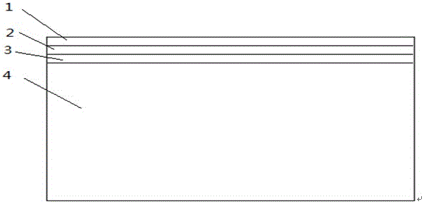
[0035] (1) if figure 1 As shown, an ITO transparent conductive film 1 with a thickness of 700-3000 angstroms is vapor-deposited on the upper surface of the p-type GaN layer 2 of the GaN-based light-emitting diode chip. The GaN-based light-emitting diode chip includes an n-type GaN layer 4 , a quantum well layer 3 and a p-type GaN layer 2 arranged from bottom to top.

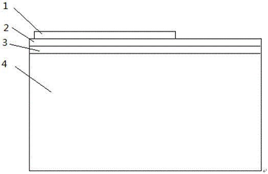
[0036] Uniform positive photoresist on the surface of the transparent conductive film 1, the thickness of the photoresist is 7000-30000 angstroms, through alignment, exposure, development and drying, and then put the chip into the ITO etching solution to corrode the mesa pattern of the transparent conductive layer (Current expansion layer graphics), that is, small table graphics, such as figure 2 Shown, rinse with water and dry, and then remove the positive photoresist.
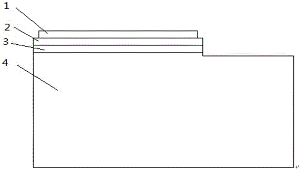
[00...


PUM

PropertyMeasurementUnit
thicknessaaaaaaaaaa
thicknessaaaaaaaaaa
thicknessaaaaaaaaaa

Abstract

The invention provides a preparation method of a GaN-based light-emitting diode chip. The method comprises the following steps: (1) growing a transparent conductive film on the surface of a p-type GaN layer and fabricating a conductive layer pattern on the surface of the transparent conductive film; (2) coating the surface of a chip with a positive photoresist and fabricating a p-type GaN table structure pattern; (3) coating the surface of the chip with a negative photoresist and fabricating a primary electrode pattern of the negative photoresist; (4) carrying out blanket exposure free of a photomask on the developed chip with the negative photoresist; (5) removing a photoresist pattern base film; (6) developing the chip and carrying out re-undercutting on the bottom part of the photoresist pattern; (7) preparing a p-type electrode and an n-type electrode to obtain the GaN-based light-emitting diode chip; and (8) fabricating a passivation layer on the surface of the GaN-based light-emitting diode chip. The method increases a process window of a contact or proximity aligner when a small line width electrode is fabricated with the negative photoresist and achieves the process that the electrode of which the line width is smaller than 4 microns is fabricated by the contact or proximity aligner.

Description

technical field [0001] The invention relates to a method for preparing a GaN-based light-emitting diode chip, which belongs to the field of optoelectronic technology. Background technique [0002] The photolithography process is to transfer the pattern on the mask plate to the chip, so that the chip has the photoresist pattern of the device you want to make, and then micro-pattern the chip. The processing method usually adopts dry etching and metal stripping. The dry etching method is ICP (Inductive Coupled Plasma, inductively coupled plasma) etching. During the ICP etching process, under the action of a high-frequency radio frequency source, the gas introduced into the chamber of the ICP etching equipment will form a plasma, and under the action of the built-in electric field, it will bombard the surface of the chip to physically etch the previous photoetching. The deposited thin film layer, while the formation of atomic groups will chemically etch the thin film layer. M...

Claims


Application Information

Patent Timeline
Patent Type & Authority Applications(China)
IPC IPC(8): H01L21/027H01L33/00
CPCH01L21/0274H01L33/0075H01L2933/0016
Inventor 马玉玲刘琦彭璐
Owner SHANDONG INSPUR HUAGUANG OPTOELECTRONICS
Why Eureka
Try Eureka