Epitaxial growth GaN thin film on metal Al substrate and preparation method of GaN thin film
An epitaxial growth and substrate technology, applied in semiconductor/solid-state device manufacturing, electrical components, circuits, etc., can solve problems such as unstable chemical properties of Al substrates, affecting the quality of epitaxial film growth, and introducing large stress into epitaxial films. , to achieve the effect of improving internal quantum efficiency, shortening nucleation time, and excellent singleness
- Summary
- Abstract
- Description
- Claims
- Application Information
AI Technical Summary
Problems solved by technology
Method used
Image


Examples
Embodiment 1
[0045] A GaN thin film 15 grown on a metal Al substrate 11 includes an Al substrate 11 , an AlN buffer layer 12 , a GaN buffer layer 13 , an amorphous AlN insertion layer 14 and a GaN thin film 15 .
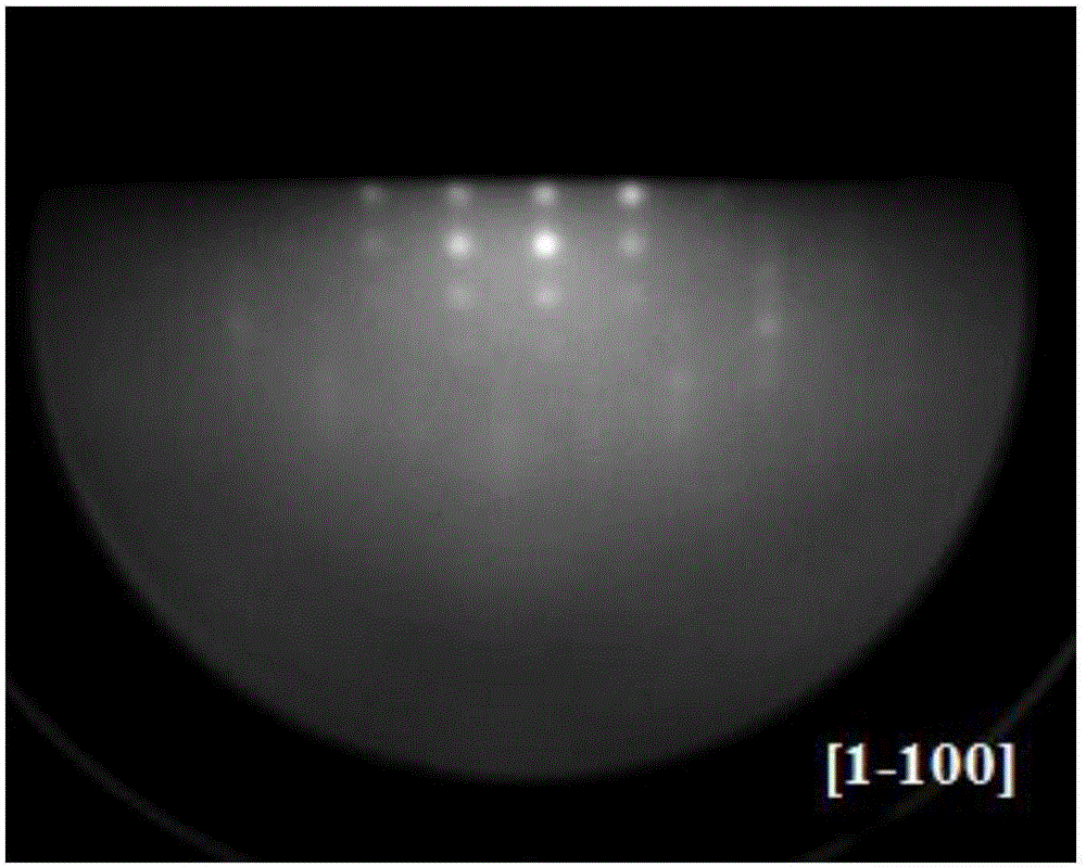
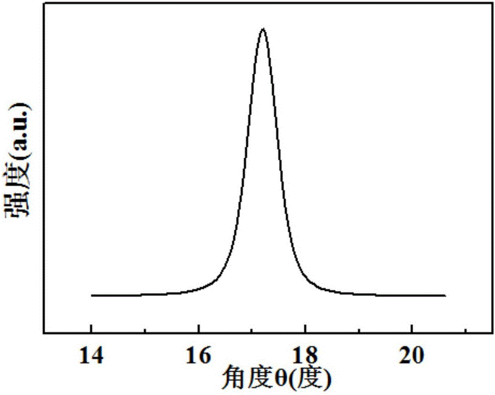
[0046] The AlN buffer layer 12 is grown on the epitaxial surface of the (111) plane of the Al substrate 11, the GaN buffer layer 13 is epitaxially grown on the AlN buffer layer 12, the amorphous AlN insertion layer 14 is grown on the GaN buffer layer 13, and the GaN thin film 15 The epitaxial growth is on the amorphous AlN insertion layer 14; the thickness of the AlN buffer layer 12 is 50nm, and the thickness of the Al substrate 11 is 0.5mm; the crystal epitaxial orientation relationship between the AlN buffer layer 12 and the GaN thin film 15 is that GaN (0001) is parallel to AlN(0001) is parallel to Al(111).
[0047] The GaN thin film 15 epitaxially grown on the metal Al substrate 11 is prepared by the following steps:
[0048] 1) Substrate selection and treatment: select meta...
Embodiment 2
[0054] A GaN thin film 15 grown on a metal Al substrate 11 includes an Al substrate 11 , an AlN buffer layer 12 , a GaN buffer layer 13 , an amorphous AlN insertion layer 14 and a GaN thin film 15 .
[0055] The AlN buffer layer 12 is grown on the epitaxial surface of the (111) plane of the Al substrate 11, the GaN buffer layer 13 is epitaxially grown on the AlN buffer layer 12, the amorphous AlN insertion layer 14 is grown on the GaN buffer layer 13, and the GaN thin film 15 The epitaxial growth is on the amorphous AlN insertion layer 14; the thickness of the AlN buffer layer 12 is 100nm, and the thickness of the Al substrate 11 is 2mm; the crystal epitaxial relationship between the AlN buffer layer 12 and the GaN thin film 15 is that GaN (0001) is parallel to AlN (0001) is parallel to Al(111).
[0056] The GaN thin film 15 epitaxially grown on the metal Al substrate 11 is prepared by the following steps:
[0057] 1) Substrate selection and treatment: select metal Al as the ...
Embodiment 3
[0063] A GaN thin film 15 grown on a metal Al substrate 11 includes an Al substrate 11 , an AlN buffer layer 12 , a GaN buffer layer 13 , an amorphous AlN insertion layer 14 and a GaN thin film 15 .
[0064] The AlN buffer layer 12 is grown on the epitaxial surface of the (111) plane of the Al substrate 11, the GaN buffer layer 13 is epitaxially grown on the AlN buffer layer 12, the amorphous AlN insertion layer 14 is grown on the GaN buffer layer 13, and the GaN thin film 15 The epitaxial growth is on the amorphous AlN insertion layer 14; the thickness of the AlN buffer layer 12 is 80nm, and the thickness of the Al substrate 11 is 1mm; the crystal epitaxial relationship between the AlN buffer layer 12 and the GaN thin film 15 is that GaN (0001) is parallel to AlN (0001) is parallel to Al(111).
[0065] The GaN thin film 15 epitaxially grown on the metal Al substrate 11 is prepared by the following steps:
[0066] 1) Substrate selection and treatment: select metal Al as the s...
PUM
| Property | Measurement | Unit |
|---|---|---|
| thickness | aaaaa | aaaaa |
| thickness | aaaaa | aaaaa |
| thickness | aaaaa | aaaaa |
Abstract
Description
Claims
Application Information
 - R&D
- Intellectual Property
- Life Sciences
- Materials
- Tech Scout
- Unparalleled Data Quality
- Higher Quality Content
- 60% Fewer Hallucinations
Browse by: Latest US Patents, China's latest patents, Technical Efficacy Thesaurus, Application Domain, Technology Topic, Popular Technical Reports.
© 2025 PatSnap. All rights reserved.Legal|Privacy policy|Modern Slavery Act Transparency Statement|Sitemap|About US| Contact US: help@patsnap.com