Wafer LED with remote fluorescent powder layer and preparation method thereof

A phosphor layer, long-distance technology, applied in the direction of electrical components, circuits, semiconductor devices, etc., can solve problems such as damage, accelerated phosphor temperature rise, disturbing chip light, etc., to achieve strong technical operability, improve light extraction efficiency, and reduce production cost effect

Active Publication Date: 2016-07-20
XIAMEN UNIV OF TECH
View PDF11 Cites 0 Cited by
  • Summary
  • Abstract
  • Description
  • Claims
  • Application Information

AI Technical Summary

Problems solved by technology

[0005] The phosphor powder is directly coated on the periphery of the chip, which means that the light emitted from the chip touches the phosphor powder. This light output mode has two disadvantages: 1. Part of the light is directly reflected back to the chip by the phosphor powder, and this part of the light disturbs the light emitted by the chip.
2. The heat generated by the chip is directly transmitted to the phosphor layer, which accelerates the temperature rise of the phosphor, directly damages and reduces the life of the phosphor, and causes LED lamp reliability problems
[0007] The existing long-distance phosphor layer coating technology is far from mature, and the unsolved problems are: 1. Phosphor layer with uniform thickness and regular shape; 2. Phosphor layer covering the light-emitting area on the side of the chip; 3. No mold Preparation of Phosphor Layer
The technical solutions that solve the above three problems at the same time often require extremely high precision and complex processes

Method used


Image

  • Wafer LED with remote fluorescent powder layer and preparation method thereof
  • Wafer LED with remote fluorescent powder layer and preparation method thereof
  • Wafer LED with remote fluorescent powder layer and preparation method thereof

Examples


Embodiment Construction

[0030] The present invention will be further described in detail below in conjunction with the accompanying drawings and embodiments. It should be understood that the specific embodiments described here are only used to explain the present invention, but not to limit the present invention. In addition, it should be noted that, for the convenience of description, only some structures related to the present invention are shown in the drawings but not all structures.

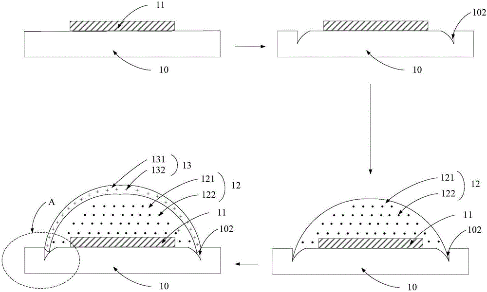
[0031] Please refer to figure 1 , a method for preparing a wafer-level LED with a remote phosphor layer, comprising the following steps:

[0032] S1, providing an LED preform, including a substrate 10 and an LED chip 11 mounted on the substrate 10;

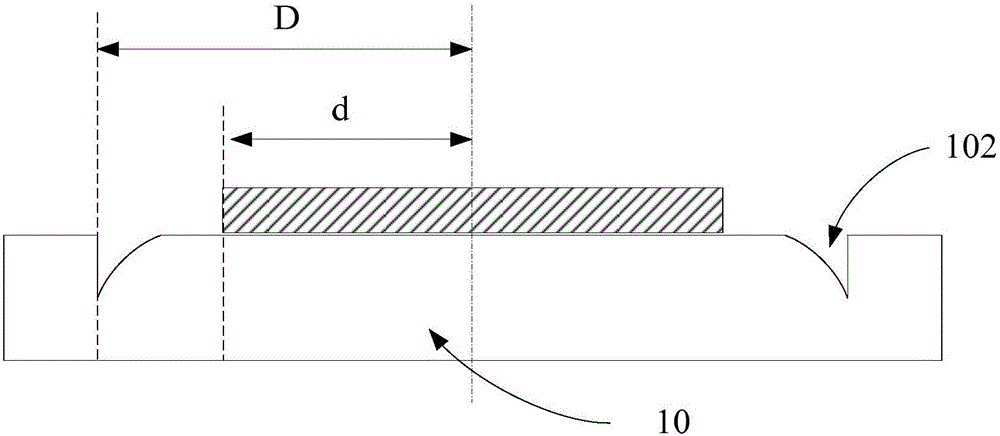
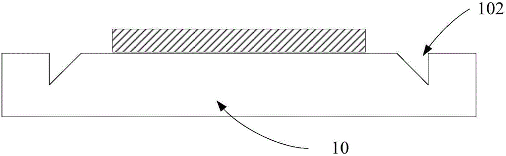
[0033] S2, forming a limiting groove 102 on the substrate 10, the limiting groove 102 surrounds the LED chip 11, and the depth of the limiting groove 102 gradually deepens along a direction away from the LED chip 11;

[0034] S3, dispensing glue for the first time a...


PUM


Abstract

The invention discloses a preparation method for a wafer light emitting diode (LED) with a remote fluorescent powder layer. The preparation method comprises the steps: providing an LED prefabricated component, including a substrate and an LED chip mounted on the substrate; forming a limit slot in the substrate, wherein the limit slot surrounds the LED chip, and the depth of the limit slot is gradually increased in a direction far away from the LED chip; carrying out first glue dispensing on the LED chip, ensuring that first dispensed glue covers the LED chip and extends to the limit slot, and after the first dispensed glue is cooled to be room temperature, solidifying the first dispensed glue to form a package lens layer; and carrying out second glue dispensing on the package lens layer, ensuring that second dispensed glue covers the package lens layer and extends to the limit slot, and after the second dispensed glue is cooled to be room temperature, solidifying the second dispensed glue to form a fluorescent powder layer, wherein the fluorescent powder layer comprises a substrate and fluorescent powders dispensed in the substrate. The invention further relates to a wafer LED with the remote fluorescent powder layer, which is obtained by the preparation method.

Description

technical field [0001] The invention relates to the technical field of LED packaging, in particular to a packaging structure of a wafer-level LED with a remote phosphor layer and a packaging method thereof. Background technique [0002] LED (LightEmittingDiode), light-emitting diode, is a solid-state semiconductor device that can directly convert electrical energy into light energy. It changes the principle of incandescent lamp tungsten filament luminescence and energy-saving lamp three-based toner luminescence, and uses electric field luminescence. The characteristics of LED are very obvious, such as long life, high luminous efficiency, low radiation and low power consumption. The spectrum of white LEDs is almost entirely concentrated in the visible light band, and its luminous efficiency can exceed 150lm / W. [0003] LED packaging refers to the packaging of light-emitting chips, which is quite different from integrated circuit packaging. The packaging of the LED is not o...

Claims


Application Information

Patent Timeline
Patent Type & Authority Applications(China)
IPC IPC(8): H01L33/48H01L33/50H01L33/54H01L33/58
CPCH01L33/48H01L33/505H01L33/54H01L33/58H01L2933/0041H01L2933/0033
Inventor 张旻澍谢安陈文哲林文倩
Owner XIAMEN UNIV OF TECH
Why Eureka
Try Eureka