G-shaped structure based dual-frequency wave-trapping ultra-wide-band antenna

An ultra-wideband antenna and notch technology, which is applied in the field of dual-frequency notch ultra-wideband antennas based on G-shaped structure, can solve the problems of complex antenna structure and process, equipment electromagnetic interference, local area network system interference, etc., and achieves simple, compact and convenient structure. Mass production, compact effect

Inactive Publication Date: 2016-07-20
HARBIN FEIYU TECH
View PDF0 Cites 2 Cited by
  • Summary
  • Abstract
  • Description
  • Claims
  • Application Information

AI Technical Summary

Problems solved by technology

[0003] However, the frequency band occupied by the current ultra-wideband communication has a common part with the wireless local area network, so it is necessary to design an antenna that can reduce the interference to the wireless local area network, and the design of ultra-wideband antennas with notch characteristics has become a current research hotspot
If there is no proper design to suppress harmonic resonance and spurious emission, the antenna will cause electromagnetic interference to nearby equipment, endangering the normal operation of the system itself and adjacent systems, especially causing interference to the currently used LAN system
Adding a filter is the most commonly used method to solve such problems, but it often causes a mismatch between the antenna and the microwave circuit, and even reduces the overall performance of the system. Therefore, a G-shaped structure-based dual-frequency notch ultra- Broadband antenna is one of the commonly used methods to solve this problem, and at the same time solve the problem that the structure and process of the current antenna are relatively complicated

Method used


Image

  • G-shaped structure based dual-frequency wave-trapping ultra-wide-band antenna
  • G-shaped structure based dual-frequency wave-trapping ultra-wide-band antenna
  • G-shaped structure based dual-frequency wave-trapping ultra-wide-band antenna

Examples


example

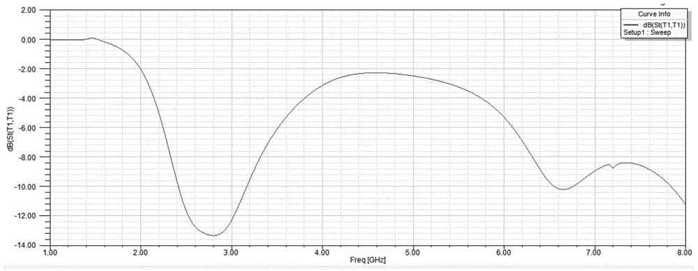
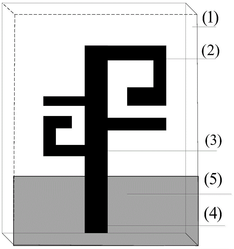
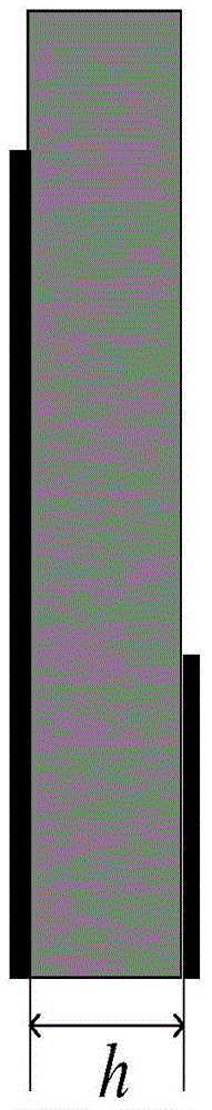
[0023] Such as figure 1 As shown, the dual-frequency notch UWB antenna based on G-shaped structure with notch characteristics includes: dielectric substrate (1), G-shaped radiation patch units (2) and (3), microstrip transmission line (4 ), ground plane (5). The radiation unit and the microstrip transmission line are all printed on the upper surface of the dielectric substrate, and the ground plane is printed on the back of the dielectric substrate. Specific dimensions: W=40mm, L=35mm, h=1.6mm, W 1 =12mm,L 1 = 15mm, W 11 = 10mm, W 12 =5mm, L 10 =19mm, L 11 = 3mm, L 12 = 2mm, L 13 = 2mm, W 2 =8.5mm, L 2 =6.8mm,W 22 =7.1mm, W 21 =3.5mm,L 20 =15mm,L 21 =2.1mm,L 22 = 1.4mm, L 23 = 1.4mm, W S = 4mm, L S = 12 mm.

[0024] The dielectric substrate is made of polytetrafluoroethylene with a thickness of 1.6 mm and a relative dielectric constant of 2.55.

[0025] The radiating unit has a G-shaped structure to realize the ultra-wideband characteristic of the antenna. ...


PUM


Abstract

The invention discloses a G-shaped structure based dual-frequency wave-trapping ultra-wide-band antenna with a wave trapping characteristic under WLAN dual-band signals. The antenna comprises a dielectric substrate (1), radiation patch units (2) and (3), a microstrip transmission line (4), and a grounding surface (5), wherein the radiation units and the microstrip transmission line are printed on the upper surface of the dielectric substrate. The antenna is compact in structure, small in size, capable of realizing the dual-band signal wave trapping characteristic, capable of adjusting the wave-trapping frequency by changing the dimensions of a C-shaped structural groove, and capable of solving the problem of same-frequency interference of an ultra-wide-band communication system.

Description

technical field [0001] The invention relates to an antenna, specifically designing a dual-frequency notch ultra-wideband antenna based on a G-shaped structure, and realizing the notch function in WLAN dual-signal frequency bands on this basis. Background technique [0002] With the rapid development of mobile communication, communication systems have higher and higher requirements for antenna bandwidth. Since the U.S. Federal Communications Commission (Federal Communications Commission) allowed the 3.1-10.6GHz frequency band to be used commercially on February 14, 2002, UWB technology has received wider attention in the academic and commercial fields, and at the same time higher requirements have been put forward for UWB antennas. requirements, making it more challenging than the design of traditional antennas, mainly in the following aspects: In addition to having an ultra-wide operating frequency band (generally 3.1GHz-10.6GHz), the antenna must also be able to maintain a ...

Claims


Application Information

Patent Timeline
Patent Type & Authority Applications(China)
IPC IPC(8): H01Q1/38H01Q1/50H01Q5/321H01Q5/25
Inventor 赵永生曹小东段瀚林
Owner HARBIN FEIYU TECH
Why Eureka
Try Eureka