Semiconductor wafer, flattening method therefor, and packaging method

A packaging method and semiconductor technology, applied in semiconductor/solid-state device manufacturing, electrical components, circuits, etc., can solve problems such as reducing alignment accuracy and packaging strength, increasing wafer spacing difference, affecting chip quality, etc., to improve cutting effect, reduce pitch difference, and improve packaging effect

Inactive Publication Date: 2016-07-27
GALAXYCORE SHANGHAI
View PDF4 Cites 13 Cited by
  • Summary
  • Abstract
  • Description
  • Claims
  • Application Information

AI Technical Summary

Problems solved by technology

[0006] For example, in the packaging process, if the wafer has a large degree of warpage (the degree of warpage is characterized by the degree of curvature of the wafer, numerically defined as the maximum value between points on the surface of the wafer in the direction perpendicular to the surface of the wafer. The height difference of the wafer; the gre

Method used


Image

  • Semiconductor wafer, flattening method therefor, and packaging method
  • Semiconductor wafer, flattening method therefor, and packaging method
  • Semiconductor wafer, flattening method therefor, and packaging method

Examples


Embodiment 1

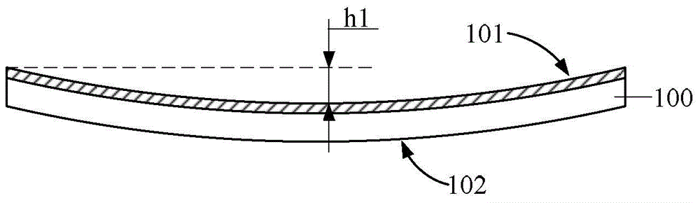
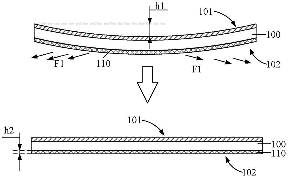
[0049] refer to figure 1 and figure 2 It is a cross-sectional view of a semiconductor wafer in different steps in this embodiment.

[0050] This implementation of the leveling method of the semiconductor wafer specifically includes:

[0051] first referencefigure 1 1. A semiconductor wafer 100 is provided, and the semiconductor wafer 100 includes a functional surface 101 formed with several semiconductor chips (not shown in the figure) and a back surface 102 opposite to the functional surface 101 .

[0052] The material of the semiconductor wafer 100 includes various materials such as silicon, germanium, gallium arsenide or silicon germanium, and semiconductor wafer materials in the art are all suitable for the semiconductor wafer in the present invention, and the present invention is for the semiconductor wafer The material is not limited.

[0053] In this embodiment, the material of the semiconductor wafer 100 is silicon.

[0054] The semiconductor wafer 100 is warped, ...

Embodiment 2

[0089] refer to Figure 5 and Figure 6 It is a cross-sectional view of a semiconductor wafer in different steps in this embodiment.

[0090] The technical scheme of the flattening method of the semiconductor wafer provided in this implementation is substantially the same as that of the semiconductor wafer flattening method provided in Embodiment 1, including: the semiconductor wafer 200 provided includes a plurality of semiconductor chips (not shown in the figure) The functional surface 201 of the functional surface 201 and the back surface 202 opposite to the functional surface 201, the semiconductor wafer 200 has warping deformation, and then a stress layer is formed on the back surface 202 of the semiconductor wafer 200 to realize the stability of the semiconductor wafer 200. leveling.

[0091] The difference between this embodiment and embodiment 1 is:

[0092] In this embodiment, before the stress layer is formed on the back surface of the semiconductor wafer 200, whe...


PUM

PropertyMeasurementUnit
Thicknessaaaaaaaaaa
Diameteraaaaaaaaaa

Abstract

The invention provides a semiconductor wafer, its leveling method and packaging method. Wherein, the flattening method of a semiconductor wafer includes: providing a semiconductor wafer, the semiconductor wafer includes a functional surface formed with several semiconductor chips and a back surface opposite to the functional surface, and the semiconductor wafer has warping deformation; Afterwards, a stress layer is formed on the back of the semiconductor wafer, and the stress layer exerts stress on the wafer, thereby reducing the absolute value of the height difference between the edge and the center of the wafer, that is, reducing the warpage of the semiconductor wafer The flatness of the semiconductor wafer can be improved to improve the packaging effect of the semiconductor wafer and the cutting effect of the semiconductor wafer, so as to improve the yield rate of each chip formed after cutting the semiconductor wafer.

Description

technical field [0001] The invention relates to the technical field of semiconductors, in particular to a semiconductor wafer, a flattening method and a packaging method thereof. Background technique [0002] Wafer Level Package (WLP) is a new packaging technology that has developed rapidly in recent years. In wafer-level packaging technology, the wafer is used as the processing object, and all semiconductor devices are completed on the wafer, and many chips are packaged, aged and tested on the wafer at the same time, and then the wafer is cut to form a single device. [0003] Compared with the traditional single-chip packaging technology, the wafer-level packaging technology eliminates the lead potting step, minimizes the package size, and makes the package size closer to the chip size; in addition, because the chip packaging, aging and testing steps are all It is carried out on silicon wafers, so the cost expenditure can be reduced through mass production. Based on the a...

Claims


Application Information

Patent Timeline
IPC IPC(8): H01L21/02H01L21/78H01L21/50H01L21/56
Inventor 赵立新蒋珂玮
Owner GALAXYCORE SHANGHAI
Why Eureka
Try Eureka