3D NAND flash memory structure and manufacturing method therefor

A manufacturing method and technology of flash memory, applied in semiconductor/solid-state device manufacturing, semiconductor devices, electrical components, etc., to achieve the effect of avoiding threshold voltage drift and leakage and improving quality

Active Publication Date: 2016-07-27
GIGADEVICE SEMICON SHANGHAI INC +1
View PDF8 Cites 8 Cited by
  • Summary
  • Abstract
  • Description
  • Claims
  • Application Information

AI Technical Summary

Problems solved by technology

[0005] In view of this, the embodiment of the present invention provides a 3D NAND flash memory structure and its manufacturing method to solve the problem in the prior art that the selection tube includes an electron trapping layer

Method used


Image

  • 3D NAND flash memory structure and manufacturing method therefor
  • 3D NAND flash memory structure and manufacturing method therefor
  • 3D NAND flash memory structure and manufacturing method therefor

Examples


Embodiment 1

[0039] Based on the above description, Embodiment 1 of the present invention provides the following solution.

[0040] figure 2 It is a schematic flow chart of the manufacturing method of the 3D NAND flash memory structure provided in the embodiment of the present invention, such as figure 2 As shown, the method may include the following steps:

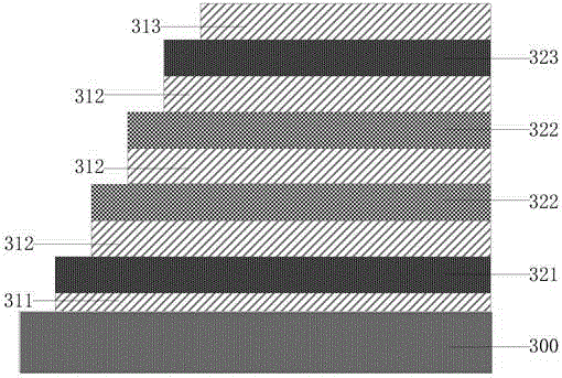
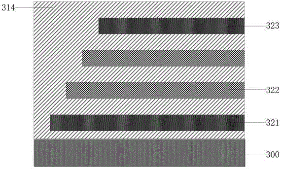
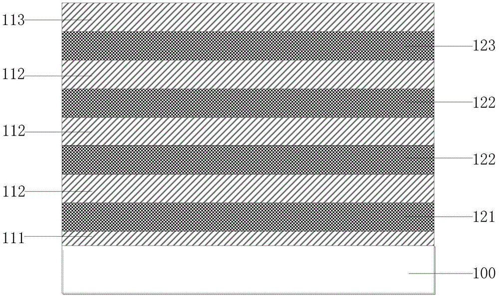
[0041] Step 21: Provide a substrate, and sequentially form a gate oxide layer, a GSL polysilicon layer, a plurality of stacked oxide dielectric layers and sacrificial dielectric layers, an SSL polysilicon layer, and a protective oxide layer on the substrate, wherein the sacrificial dielectric layer layers are formed between adjacent oxide dielectric layers;

[0042] Step 22, etching to form a cylindrical channel exposing the substrate;

[0043] Step 23, sequentially forming a tunnel oxide layer, polysilicon and a polysilicon isolation dielectric layer in the cylindrical trench;

[0044] Step 24, etching to form a source trench e...


PUM


Abstract

The invention relates to the technical field of semiconductor manufacturing, in particular to a 3D NAND flash memory structure and a manufacturing method of the 3D NAND flash memory structure. The method includes: providing a substrate, and sequentially forming a gate oxide layer, a source selection transistor polysilicon layer, a plurality of stacked oxide dielectric layers and sacrificial dielectric layers, a drain selection transistor polysilicon layer, and a protective oxide layer on the substrate ; Etching to form a cylindrical channel that exposes the substrate; forming a tunnel oxide layer, polysilicon and polysilicon isolation dielectric layer in the cylindrical channel; etching to form a source trench that exposes the substrate, and forming a common source removing the sacrificial dielectric layer by wet etching; forming an electron trapping layer and a blocking oxide layer on the side walls of the source trench and the inner wall of the oxide dielectric layer; forming a gate on the surface of the blocking oxide layer. The selection tube prepared by the method does not include electron trapping layer silicon nitride, avoids threshold voltage drift and leakage phenomenon of the selection tube, and improves the quality of the memory device.

Description

technical field [0001] The invention relates to the technical field of semiconductor manufacturing, in particular to a 3D NAND flash memory structure and a manufacturing method of the 3D NAND flash memory structure. Background technique [0002] With the rapid development of flash memory, the three-dimensional (3D) flash memory structure has been developed rapidly, and 3D NAND flash memory has been widely used in semiconductor devices. [0003] In the manufacturing method of existing 3D NAND flash memory structure, the manufacturing process of the drain selection transistor (StringSelectLine, SSL) and the source electrode selection transistor (GroundSelectLine, GSL) is consistent with the manufacturing process of the memory cell, that is, the gate of the selection transistor is formed In the process of oxidation (GateOxide) layer, it is inevitable to introduce electron trapping layer (ChargeTrapLayer) silicon nitride SiN into the selection tube. The selection tube includes ...

Claims


Application Information

Patent Timeline
Patent Type & Authority Applications(China)
IPC IPC(8): H01L21/8247H01L27/115
Inventor 熊涛刘钊许毅胜舒清明
Owner GIGADEVICE SEMICON SHANGHAI INC
Why Eureka
Try Eureka