K-wave band microstrip patch antenna array

A technology of microstrip patch antenna and microstrip antenna, which is applied in the directions of antenna array, antenna, antenna coupling, etc., can solve the problem of weak anti-interference ability of antenna and detection, and achieve the effects of high sensitivity, increased bandwidth, and accurate azimuth

Inactive Publication Date: 2016-07-27
GUILIN UNIV OF ELECTRONIC TECH
2 Cites 12 Cited by

AI-Extracted Technical Summary

Problems solved by technology

[0004] The present invention needs to solve the problem that the existing K-band microstrip array antenna has w...

Method used

A kind of K wave band microstrip patch antenna array, the dielectric plate is provided with mutually parallel and identical structure 3 column antennas, is respectively transmitting antenna (1), the first receiving antenna (2) and the second receiving antenna (3) , the transmitting antenna (1) is arranged opposite to the first receiving antenna (2) and the second receiving antenna (3); the dielectric plate is arranged as a rectangle or a square, and when the dielectric plate is rectangular, its size is (48 × 62) mm, The user can also adjust the size according to the needs. The dielectric board is made of non-conductive non-metallic material; metallized grounding holes (7) are set around the dielectric board, and the bottom of the dielectric board is provided with a metal grounding plate (9), and the grounding plate (9) ) is provided with a grounding port (11) around, wherein the grounding hole (7) and the grounding port (11) correspond to each other, which facilitates the subsequent increase of the circuit control system grounding, and correspondingly increases the bandwidth of the antenna, as shown in Figure 1 and Figure 2 shown.
Each column antenna array is provided with 8 microstrip antenna units (5), a multi-channel power divider (6) and feed port (4); There are several impedance converters ( 6.1) and several feeder bending lines (6.2), and the microstrip transmission line (6.3) that plays a connecting role; each microstrip antenna unit 5 in the antenna of the same column is connected to each output port of the power divider (6) It is connected through the feeding bent line (6.2); in the existing technology, the smooth straight line connection is used. When setting the unit spacing, in order to ensure the consistency of the phase, the spacing between the units will inevitably be relatively large, which is prone to grid failure. Lobe, which affects the overall radiation performance of the antenna, the use of the meander line can effectively control the distance between the units under the premise of ensuring phase consistency. Adjacent microstrip antenna units (5) are connected by impedance transformers (6.1) and microstrip transmission lines (6.3); the microstrip antenna units 5 of each column antenna are arranged on the same straight line; the microstrip antennas of each column antenna From the middle to both sides of the unit (5), the spacing between the microstrip antenna units (5) gradually increases, and the distance between the microstrip antenna units (5) is equidistant, and the ideal antenna sidelobe level cannot be obtained ; By gradually increasing the distance between the elements from the middle to both sides, the sidelobe level of the antenna is less than or equal to -20dB, so that the anti-interference ability of the antenna is enhanced; the microstrip antenna unit (5) is a microstrip patch antenna, and the power distribution The device (6) has multi-path power distribution and is connected with the microstrip antenna unit (5), so as to realize the control of the input power of each different antenna unit, so as to meet the design requirements. The number of microstrip antenna units (5) in each row of antennas can be changed according to specific requirements in actual engineering. It is generally an even number, so that the radiation patterns of the transmitting and receiving antennas are perpendicular to the medium plane, as shown in Figure 1.
The number of microstrip antenna unit (5) can increase or decrease along with the demand of user, increase or decrease with the number of double number, the increase of microstrip antenna unit (5), antenna radiation gain increases , the radiation distance is farther under the control of the control circuit,...

Abstract

The invention provides a K-band microstrip patch antenna array, which belongs to the field of antennas. The dielectric board is provided with three columns of antennas parallel to each other and with the same structure, which are respectively transmitting antennas, first receiving antennas and second receiving antennas; the antennas of each column There are several microstrip antenna units, several 1/4 wavelength microstrip feeders, power dividers and feed ports; there are several impedance converters, several microstrip transmission lines and several feeder bending lines in the power divider ; The bottom of the dielectric plate is provided with a metal grounding plate; the invention designs a K-band microstrip array antenna with stronger anti-interference ability, so that the detection of moving objects is more accurate.

Application Domain

Antenna arraysRadiating elements structural forms +3

Technology Topic

Wave bandMicrostrip patch antenna array +7

Image

  • K-wave band microstrip patch antenna array
  • K-wave band microstrip patch antenna array

Examples

  • Experimental program(1)

Example Embodiment

[0021] Hereinafter, the present invention will be further described in conjunction with the embodiments.
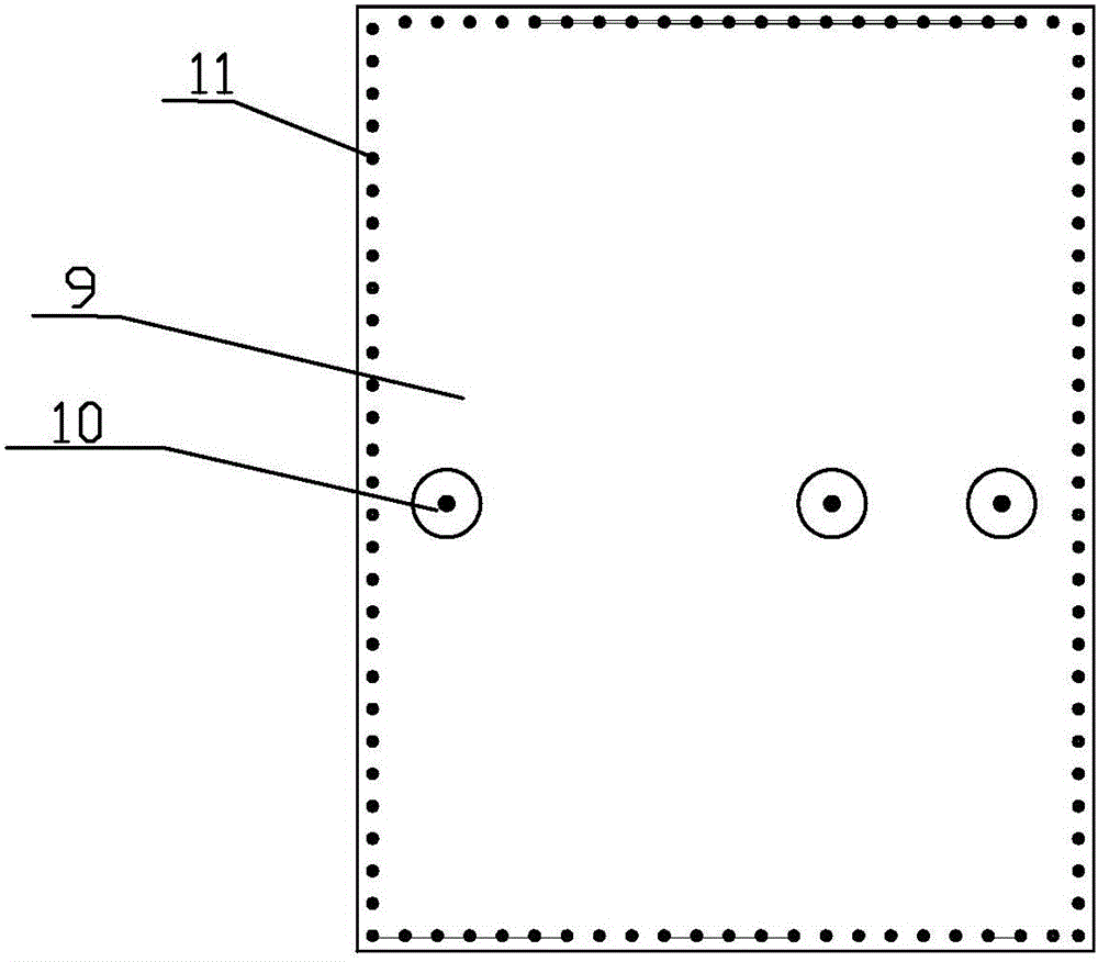
[0022] A K-band microstrip patch antenna array. Three antennas parallel to each other and with the same structure are arranged on a dielectric board. They are a transmitting antenna (1), a first receiving antenna (2) and a second receiving antenna (3). The transmitting antenna (1) Set opposite to the first receiving antenna (2) and the second receiving antenna (3); the dielectric plate is set to be rectangular or square. When the dielectric plate is rectangular, its size is (48×62) mm, and the user can also Adjust the size as needed. The dielectric plate is made of non-conductive non-metallic materials; metalized grounding holes (7) are set around the dielectric plate, a metal ground plate (9) is provided at the bottom of the dielectric plate, and the ground plate (9) is provided around the There is a grounding port (11), where the grounding hole (7) and the grounding port (11) correspond to each other, which facilitates the subsequent increase of the circuit control system grounding, and correspondingly increases the bandwidth of the antenna, such as figure 1 , figure 2 Shown.
[0023] In order to reduce the mutual interference of the feed ports of the transmitting and receiving antenna array and improve the isolation between each other, the transmitting antenna (1) and the first receiving antenna (2) are 11mm apart from the first receiving antenna under the premise of minimizing the overall size of the antenna. The distance between the two receiving antennas (3) is 17mm, and the distance between the first receiving antenna (2) and the second receiving antenna (3) is 6mm.
[0024] Grounding holes (11) are provided around the grounding plate (9). The grounding holes (11) through the grounding holes (7) are the same through holes corresponding to the front and back. In order to minimize the loss and meet the minimum size of the actual processing, the grounding hole The inner diameter of the hole is set to 3mm, and the outer diameter of the hole is 6mm.
[0025] Each column of antenna array is provided with 8 microstrip antenna units (5), a multi-channel power divider (6) and feed port (4); there are several impedance converters (6.1) and Several feeding bending lines (6.2), as well as a microstrip transmission line (6.3) for connection; each microstrip antenna unit 5 in the same column of antennas is fed with each output port of the power divider (6) Bending line (6.2) connection; in the existing technology, smooth straight line connection is used. When setting the cell spacing, in order to ensure the consistency of the phase, the spacing between the cells will inevitably be large, and grating lobes are prone to appear. Influencing the overall radiation performance of the antenna, the use of a bent line can effectively control the spacing between the units while ensuring phase consistency. The adjacent microstrip antenna units (5) are connected by an impedance converter (6.1) and a microstrip transmission line (6.3); the microstrip antenna unit 5 of each antenna column is arranged on the same straight line; the microstrip antenna of each antenna column From the middle to both sides of the unit (5), the distance between the microstrip antenna units (5) gradually increases, and the distance between the microstrip antenna units (5) is equidistant, and the ideal antenna sidelobe level cannot be obtained. ; Through the design of gradually increasing the distance between the elements from the middle to the two sides, the sidelobe level of the antenna is less than or equal to -20dB, so that the anti-interference ability of the antenna is enhanced; the microstrip antenna unit (5) is a microstrip patch antenna with power distribution The device (6) has multi-path power distribution and is connected with the microstrip antenna unit (5) to realize the control of the input power of each different antenna unit, thereby meeting the design requirements. The number of microstrip antenna units (5) in each column of antennas can be changed, depending on the specific requirements in the actual project. Generally double numbers, so that the radiation pattern of the transmitting and receiving antennas is perpendicular to the plane of the medium, such as figure 1 Shown.
[0026] The distance between the antenna units (5) is gradually increased, which can effectively reduce the sidelobe compared with the equal or smaller distance, thereby reducing clutter interference and improving the antenna receiving sensitivity. The main purpose is to adjust the sidelobe, so that it can reduce the sidelobe more effectively when the power allocation ratio is determined, so that the ability to resist clutter interference is stronger. In terms of directivity requirements, it can also be radiation at different angles, which should be designed according to actual application requirements, so that the detection of targets at different angles can be achieved.
[0027] In the antennas of the same column, the feed port 4 is set at the midpoint of the antennas in each column, and the upper and lower microstrip antenna units 5 of the feed port (4) pass through the 1/4 wavelength microstrip feeder (8) and the power divider ( 6) The two output ports are connected; the other microstrip antenna units (5) are connected to the output ports of the power splitter (6) through the 1/4 wavelength microstrip feeder 8 and the feed bending line (6.2); bending line (6.2) is to ensure the consistency of the phase under the condition that the unit spacing gradually increases, so that the maximum gain is ensured in the vertical direction of the antenna plane. If there is no bending line, if the phase consistency is to be ensured, the spacing between the antennas will inevitably be increased, causing the radiation pattern to produce grating lobes, and the radiation power cannot be concentrated on the main lobe, which affects radiation efficiency and receiving sensitivity. The feed bending line (6.2) ensures to a certain extent that the adjustment of the unit spacing within a certain range will not affect the antenna performance.
[0028] The number of microstrip antenna units (5) can be increased or decreased in accordance with the needs of users. The number of microstrip antenna units (5) increases or decreases. The increase of the microstrip antenna unit (5) increases the antenna radiation gain and the radiation distance. It is farther under the control of the control circuit, so as to meet the detection of the longer distance of the vehicle when the vehicle speed is faster, so as to prompt the owner to make the corresponding adjustment to the vehicle speed. And this design adds a microstrip antenna array to receive signals, so that the system can not only detect the speed and distance of the moving object, but also the position of the moving object. It makes the judgment of moving objects more accurate and greatly reduces the probability of danger; with the increase of the microstrip antenna unit (5), the board surface is slightly enlarged. In order not to affect the installation of the antenna, the size of the original design is (48×62) )mm, which is better for the automotive collision avoidance radar system.
[0029] The feed port (4) is set at the midpoint of the antenna in each column, and the input impedance of the feed port (4) is set to several commonly used ones. The back-fed pin feed is adopted, and the antenna array feed network is through the microstrip transmission line Each microstrip antenna unit is fed, and each array of antenna arrays are fed separately, and a certain distance is set between each other to improve the isolation between the antenna arrays and reduce the mutual influence.
[0030] The design is mainly based on the dual-path branch feed of the power divider (6), which is based on the feed mode of the combination of series and parallel, and the spacing between the microstrip antenna units (5) gradually increases. It can also be designed in the form of a unilateral series-fed antenna array, and the series-fed method is used to meet the product design index requirements. The microstrip antenna unit (5) and the microstrip antenna unit (5) are connected through a microstrip transmission line and impedance The converter (6.1) is directly connected. Both bilateral feeding and unilateral feeding have their own advantages and disadvantages. The double-sided feed design is divided into two symmetrical channels by the power divider (6). In the actual design simulation, due to the symmetrical structure, the design process is simplified during the design and time is saved. However, the structure is more than simple Side cross-feeding is complicated, and there are many microstrip lines, so the energy loss increases accordingly, and the radiated power decreases, which affects the antenna performance. Since the antenna unit of the single-side series feeder is also a part of the transmission line, the structure is relatively simple, the transmission line loss is reduced compared with the double-side feed, and the radiation efficiency is increased; but it is because of the simple structure, for each of them The impedance converter has higher matching requirements, which makes the current amplitude of each antenna unit different. When designing, the amount of parameter change increases, the design difficulty increases correspondingly, and the design time extends, which will be disadvantaged in the competition.
[0031] The microstrip array antenna proposed in this design can be directly used for vehicle flow detection, traffic monitoring, traffic light control, etc. in the 24GHz frequency band. It can also be used for security intrusion detection, parking space detection and microwave communication systems working in the 24GHz frequency band. In addition, this design pattern can provide design reference for microstrip array antennas in other microwave frequency bands.
[0032] The proposal of this design has carried out simulation and physical processing test. In order to ensure that the application requires an antenna sidelobe level less than or equal to -20dB, a certain margin is given to the theoretically calculated sidelobe level in the design, which is selected as -25dB. In consideration of reducing the influence of process errors on the design, the minimum used line width and spacing are particularly restricted. Taking into account the accuracy of the theoretical calculation model, several theoretical derivations and more reasonable approximations have been made to the critical impedance calculation. At the same time, the maximum used line width is limited, which helps to ensure the accuracy of the calculation model and reduce parasitic effects. According to the rationality of the antenna pattern, beam width, sidelobe level, maximum and minimum line width predicted by theory, it is easy to judge whether the design goal has been reached, and how to adjust the design parameters when the design goal is not reached. And through physical testing, the experimental verification of theoretical design and simulation is completed, and the index requirements are met through debugging and modification.
[0033] The preferred embodiments of the present invention have been described in detail above, but the present invention is not limited to the embodiments. Those skilled in the art can also make various equivalent modifications or substitutions without departing from the spirit of the present invention. All these equivalent modifications or replacements are included in the scope of the present application.

PUM

no PUM

Description & Claims & Application Information

We can also present the details of the Description, Claims and Application information to help users get a comprehensive understanding of the technical details of the patent, such as background art, summary of invention, brief description of drawings, description of embodiments, and other original content. On the other hand, users can also determine the specific scope of protection of the technology through the list of claims; as well as understand the changes in the life cycle of the technology with the presentation of the patent timeline. Login to view more.

Similar technology patents

Instrument for exploring fractures and cavernouse formation

InactiveCN1680828AImprove resolution and accuracyImprove anti-interference ability
Owner:中国人民解放军沈阳军区司令部工程科研设计所

Built in gas flow meter and temperature pressure compensation transmission method

ActiveCN1479083AShield signal interferenceImprove anti-interference ability
Owner:上海埃科燃气测控设备有限公司

High-accuracy single F-P plate angular displacement measurement instrument

Owner:SHANGHAI INST OF OPTICS & FINE MECHANICS CHINESE ACAD OF SCI

Classification and recommendation of technical efficacy words

  • Improve anti-interference ability
  • high sensitivity

Composite electromagnetic shielding paint based on nano carbon material

InactiveCN105331264AImprove anti-interference abilityGood protection against electromagnetic radiation
Owner:INST OF URBAN ENVIRONMENT CHINESE ACAD OF SCI

System and method for optical coherence imaging

ActiveUS20060055936A1sufficient signal to noise ratiohigh sensitivity
Owner:THE GENERAL HOSPITAL CORP

Three-axis integrated MEMS accelerometer

InactiveUS20060272413A1low costhigh sensitivity
Owner:VAGANOV VLADIMIR +1

Patterning process, resist composition, and acetal compound

InactiveUS20110236826A1high dissolution contrasthigh sensitivity
Owner:SHIN ETSU CHEM CO LTD
Why Eureka
Try Eureka