Light-operated terahertz modulator based on graphene/silicon-doped compound double-layer structure

A composite double-layer, graphene technology, applied in the field of terahertz wave applications, can solve the problems that cannot meet the needs of high-speed modulation, and the modulation rate is only on the order of kHz, so as to improve power utilization, increase modulation depth, and increase modulation amplitude Effect

CN105824138AActive Publication Date: 2016-08-03UNIV OF ELECTRONICS SCI & TECH OF CHINA
5 Cites 18 Cited by

Patent Information

Authority / Receiving Office
CN · China
Patent Type
Applications(China)
Current Assignee / Owner
Publication Date
2016-08-03

Smart Images

  • Figure 1
    Figure 1
  • Figure 2
    Figure 2
  • Figure 3
    Figure 3
Patent Text Reader

Abstract

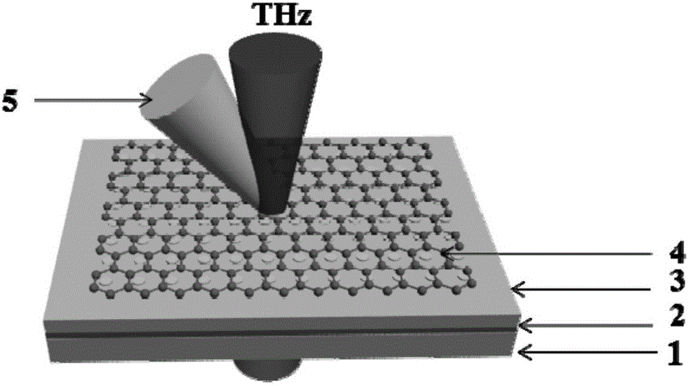
The invention belongs to the technical field of terahertz wave application and provides a light-operated terahertz modulator based on a graphene / silicon-doped compound double-layer structure. The light-operated terahertz modulator is used for simultaneously acquiring large modulation rate and modulation depth and comprises a substrate 1, an insulating layer 2, a metal doping Si semiconductor layer 3, a graphene film 4 and a pumping laser beam 5 which are successively arranged from bottom to top. The light-operated terahertz modulator is characterized in that the metal doping Si semiconductor layer 3 and the graphene film 4 form the graphene / silicon-doped compound double-layer structure. The light-operated terahertz modulator provided by the invention has the characteristics of high speed, broadband, large-amplitude modulation and room-temperature work, can work under the conditions of 0.2-2.6THz, the modulation frequency being 10MHz and the maximum modulation depth being 50% and above, and can be applied to a terahertz high-speed wireless communication system and also can be used as a high-speed broadband terahertz wave modulator in a plurality of application systems for terahertz imaging and detection.
Need to check novelty before this filing date? Find Prior Art

Description

technical field

[0001] The invention belongs to the technical field of terahertz wave applications, and provides a terahertz modulation device, specifically a light-controlled terahertz modulator based on a graphene / doped silicon composite double-layer structure. Background technique

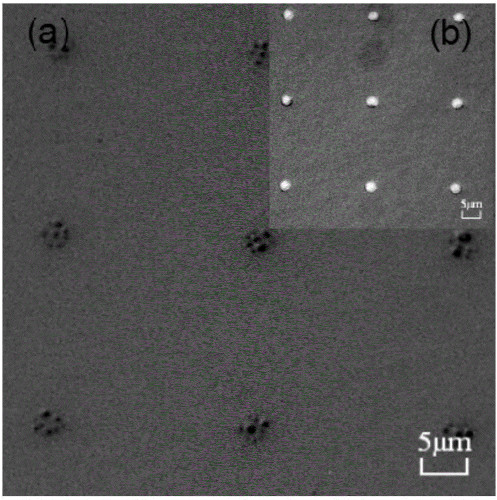
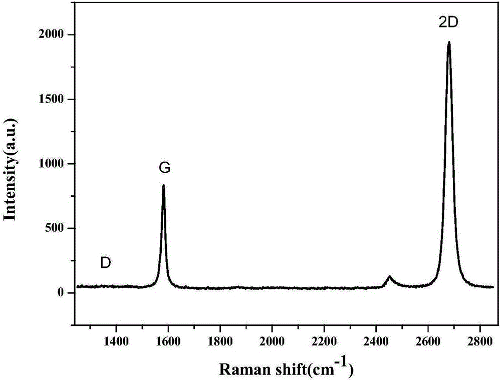
[0002] Terahertz wave (THz) refers to electromagnetic waves with a frequency in the range of 0.1THz-10THz (wavelength 0.03-3mm). Its band is located between microwave and infrared waves, and occupies an important position in the electromagnetic spectrum. the transition area. Terahertz waves have very important applications in the fields of wireless communication, non-destructive detection, security inspection, and radar imaging. In the terahertz application system, active control devices (activedevices) can realize a series of functions such as modulation, switching, attenuation, and steering of the terahertz beam, and are the core components of the construction of the terahertz application s...

Examples

Embodiment Construction

[0025] The present invention will be further described below with reference to the accompanying drawings.

[0026] In this embodiment, an optically controlled terahertz wave modulator based on a "graphene / doped Si semiconductor" composite double-layer structure is provided, and its structure is as follows figure 1 As shown, it includes a substrate 1 , an insulating layer 2 , a gold lattice doped semiconductor layer 3 , a graphene film 4 and a pumping laser beam 5 arranged sequentially from bottom to top. In this embodiment, an SOI substrate is used, that is, the substrate is a sapphire substrate with a thickness of 400 μm, and the insulating layer is SiO with a thickness of about 200 nm. 2 , Si semiconductor is intrinsic N-type high-resistance Si, its resistivity is greater than 1000Ω / cm, thickness is 50μm, doped metal is Au, doping type is lattice doping, and its gold point distribution is as follows figure 2 As shown, it should be noted that the metal dots in lattice dopin...