
Recovery circuit for improving negative bias-temperature instability of memory clock circuit

A technology of negative bias temperature and recovery circuit, which is applied in the direction of static memory, digital memory information, information storage, etc., can solve the problems of clock frequency, reading and writing speed drop, unable to end the circuit in time, MP1 performance degradation, etc., to reduce internal The effect of widening the effective pulse, reducing the NBTI effect, and reducing the working time

Active Publication Date: 2016-08-03
SUZHOU XIANLIN LIQI ELECTRONICS TECH
View PDF3 Cites 11 Cited by
  • Summary
  • Abstract
  • Description
  • Claims
  • Application Information

AI Technical Summary

Problems solved by technology

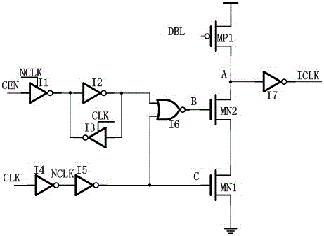
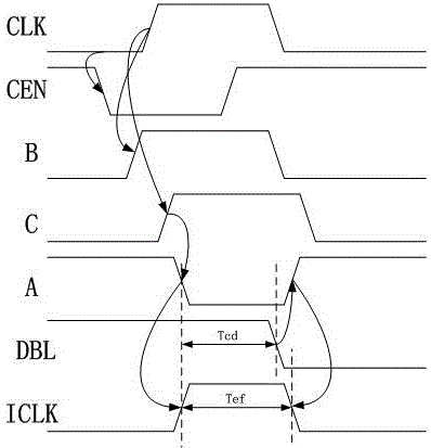
Under long-term high-frequency work, the negative bias between the gate and source of MP1 will cause NBTI effect, and the performance of MP1 will be degraded, causing the falling edge of ICLK to slow down, and the internal work of the circuit cannot be completed in time. On the one hand, clock frequency, read and write speed will therefore decrease, on the other hand, it will cause an increase in circuit power consumption

Method used


Image

  • Recovery circuit for improving negative bias-temperature instability of memory clock circuit
  • Recovery circuit for improving negative bias-temperature instability of memory clock circuit
  • Recovery circuit for improving negative bias-temperature instability of memory clock circuit

Examples


Embodiment Construction

[0022] The present invention will be described in detail below with reference to the accompanying drawings and in combination with embodiments.

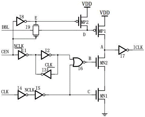
[0023] refer to figure 2 As shown, a recovery circuit for improving the temperature instability of the negative bias voltage of the memory clock circuit, the circuit includes a clock input circuit and a recovery circuit for the NBTI effect;

[0024] The clock input circuit includes an enabling signal terminal CEN, a clock signal terminal CLK, inverters I1, I2, I3, I4, I5, I7, a NOR gate I6, a PMOS transistor MP1, and an NMOS transistor MN1 and MN2. The energy signal terminal CEN is connected to the input terminal of the inverter I1, the output terminal of the inverter I1 is respectively connected to the input terminal of the inverter I2 and the output terminal of the inverter I3, and the output terminal of the inverter I2 is connected to the output terminal of the inverter I3 The input ends of the inverters are connected to the fir...


PUM


Abstract

The invention discloses a recovery circuit for improving the negative bias-temperature instability of a memory clock circuit. The recovery circuit comprises an enable signal terminal CEN, a clock signal terminal CLK, phase inverters I1, I2, I3, I4, I5, and I7, NOR gate I6, PMOS tube MP1, and NMOS tubes MN1 and MN2, and also comprises a recovery circuit with a NBTI effect. The recovery circuit with a NBTI effect comprises a PMOS tube MP2, a phase inverter I8, and a transmission gate I9. The source electrode of MP2 is connected to a high level terminal VDD, the drain electrode of MP2 is connected to the grid electrode of the MP1 tube, the grid electrode of MP2 is connected to the output terminal of the phase inverter I8 and NMOS grid terminal of transmission gate I9, the input terminal of the phase inverter I8 is connected to the enable signal terminal CEN and the PMOS grid terminal of transmission gate I9, one end of transmission gate I9 is connected to the grid electrode of MP1, and the other end is connected to a virtual bit line DBL. The provided recovery circuit can reduce the influence of NBTI effect on PMOS tube in the circuit so as to guarantee the highest work frequency of circuit and low energy consumption performance.

Description

technical field [0001] The invention belongs to the technical field of embedded memory, and relates to a recovery circuit for improving the temperature instability of negative bias voltage of an embedded memory clock input circuit. Background technique [0002] Advances in modern semiconductor technology have brought about reductions in transistor size and supply voltage. However, after the process reaches 65nm, process deviations caused by random doping can have a bad impact on circuit performance. At the same time, in order to meet the requirements of modern high-performance electronic systems, the integration level of embedded memory is getting higher and higher, and the operating frequency is also increasing, and the highest has reached several gigahertz (GHz), which is very important for transistors. high reliability requirements. In traditional circuit design, designers assume that the electrical and physical characteristics of transistors are deterministic and predi...

Claims


Application Information

Patent Timeline
Patent Type & Authority Applications(China)
IPC IPC(8): G11C7/04G11C7/10
CPCG11C7/04G11C7/1006
Inventor 刘海齐
Owner SUZHOU XIANLIN LIQI ELECTRONICS TECH
Learn More