Accumulation vertical HEMT device

It is an accumulation type and device technology, which is applied in the direction of semiconductor devices, electrical components, circuits, etc. It can solve the problems of increasing the on-resistance of the device and limiting the forward current capability of the device, so as to reduce the on-resistance and improve the forward current drive. Capability, the effect of uniform electric field distribution

Active Publication Date: 2016-08-10
UNIV OF ELECTRONICS SCI & TECH OF CHINA
View PDF4 Cites 17 Cited by
  • Summary
  • Abstract
  • Description
  • Claims
  • Application Information

AI Technical Summary

Problems solved by technology

[0004] For conventional vertical GaN HEMTs, vertical devices cannot use 2DEG to achieve conduction, and the conduction current needs to flow through the buffer layer, which makes the on-resistance much higher than that of lateral devices; and the device mainly relies on the p-GaN current blocking layer and n -The PN junction formed between the GaN buffer layers is used to withstand the withstand voltage. In order to achieve a high breakdown voltage, the concentration of the n-GaN buffer layer should not be too high, but a low-concentration buffer layer will increase the on-resistance of the device, which greatly limits Therefore, conventional vertical GaNHEMT devices have a contradictory relationship between withstand voltage and on-resistance

Method used


Image

  • Accumulation vertical HEMT device
  • Accumulation vertical HEMT device
  • Accumulation vertical HEMT device

Examples


Embodiment 2

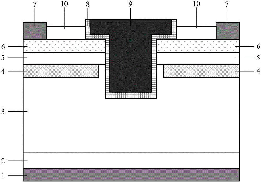
[0033] Compared with Embodiment 1, the insulating gate dielectric 8 of the device in this example presents a stepped shape, and other structures are the same as in Embodiment 1, such as Figure 4 shown. The introduction of the step-shaped insulating gate dielectric 8 can effectively reduce the gate capacitance and improve the dynamic performance of the device, but the accumulation effect of the gate will be weakened.

Embodiment 3

[0035] Compared with Embodiment 1, the insulated gate structure of the device in this example is a split insulated gate structure, and other structures are the same as in Embodiment 1, such as Figure 5 shown. Adopting the split insulated gate electrode structure can effectively reduce the gate-drain capacitance, thereby improving the dynamic performance of the device; at the same time, a new electric field peak is introduced at the interface between the gate electrode 91 and the split gate electrode 92, thereby improving the electric field distribution in the drift region and improving Device withstand voltage. In addition, the potential of the split gate electrode 92 may be positive potential, negative potential, or zero potential.

Embodiment 4

[0037]Compared with Embodiment 1, the current blocking layer 4 of the device of this example is composed of multiple P-type doped blocking layers parallel to each other in the vertical direction and having the same size, and other structures are the same as in Embodiment 1, such as Figure 6 shown. The introduction of a multi-layer P-type doped barrier layer can effectively improve the electric field distribution of the buffer layer, increase the average electric field intensity, and improve the withstand voltage of the device; in addition, due to the depletion effect of the P-type doped barrier layer on the buffer layer, it can be Increase the doping concentration of the buffer layer to a certain extent, thereby reducing the on-resistance of the device and improving the forward current output capability.


PUM


Abstract

The invention belongs to the technical field of semiconductors, and relates to an accumulation vertical HEMT device. In the forward conduction state of the accumulation vertical HEMT device, a high-concentration electron accumulation layer is formed at the side wall of an insulated gate electrode structure so that conduction resistance of the device can be greatly reduced and the device is ensured to have great forward current driving capacity; and in the reverse blocking state, the effect of electric field concentration of the interface of the barrier layer and the buffer layer of the device can be effectively improved by the insulated gate electrode structure, and a new electric field peak is introduced to the tail end of the insulated gate electrode structure so that electric field distribution is enabled to be more uniform, and off-state breakdown voltage of the device can be enhanced. The preparation technology of the device is compatible with the conventional technology.

Description

technical field [0001] The invention belongs to the technical field of semiconductors, and relates to an accumulation type vertical HEMT (High Electron Mobility Transistor, high electron mobility transistor) device. Background technique [0002] The existing high withstand voltage GaN HEMT structure is mainly a lateral device, and the basic structure of the device is as follows figure 1 shown. The device mainly includes a substrate, a GaN buffer layer, an AlGaN barrier layer, and a source, a drain, and a gate formed on the AlGaN barrier layer. The barrier layer forms a Schottky contact. However, for lateral GaN HEMTs, in the cut-off state, electrons injected from the source can pass through the GaN buffer layer to reach the drain, forming a leakage channel. Excessive buffer layer leakage current will cause early breakdown of the device and cannot fully utilize the GaN HEMT. The high withstand voltage advantage of the material limits the application of GaN HEMTs in high vo...

Claims


Application Information

Patent Timeline
Patent Type & Authority Applications(China)
IPC IPC(8): H01L29/778H01L29/423
CPCH01L29/4236H01L29/7786H01L29/7788
Inventor 罗小蓉杨超吴俊峰彭富魏杰邓思宇张波
Owner UNIV OF ELECTRONICS SCI & TECH OF CHINA
Why Eureka
Try Eureka