LDMOS device structure and manufacture method thereof

A technology of device structure and manufacturing method, which is applied in semiconductor/solid-state device manufacturing, semiconductor devices, electrical components, etc., can solve the problem of inability to achieve lithography size, etc., to solve the problem of lithography alignment accuracy, manufacturing yield and uniformity The effect of sexual security

Inactive Publication Date: 2016-08-10
KUNSHAN HUATAI ELECTRONICS TECH CO LTD
View PDF6 Cites 6 Cited by
  • Summary
  • Abstract
  • Description
  • Claims
  • Application Information

AI Technical Summary

Problems solved by technology

In addition, concentrated boron implantation and long-term annealing form the connection between the source surface and the substrate. Long-term high temperature will cause large warping of the silicon wafer, and the lithography size below 0.25um cannot be achieved.

Method used


Image

  • LDMOS device structure and manufacture method thereof
  • LDMOS device structure and manufacture method thereof
  • LDMOS device structure and manufacture method thereof

Examples


Embodiment Construction

[0035] The present invention will be further described below in conjunction with the accompanying drawings. The following examples are only used to illustrate the technical solution of the present invention more clearly, but not to limit the protection scope of the present invention.

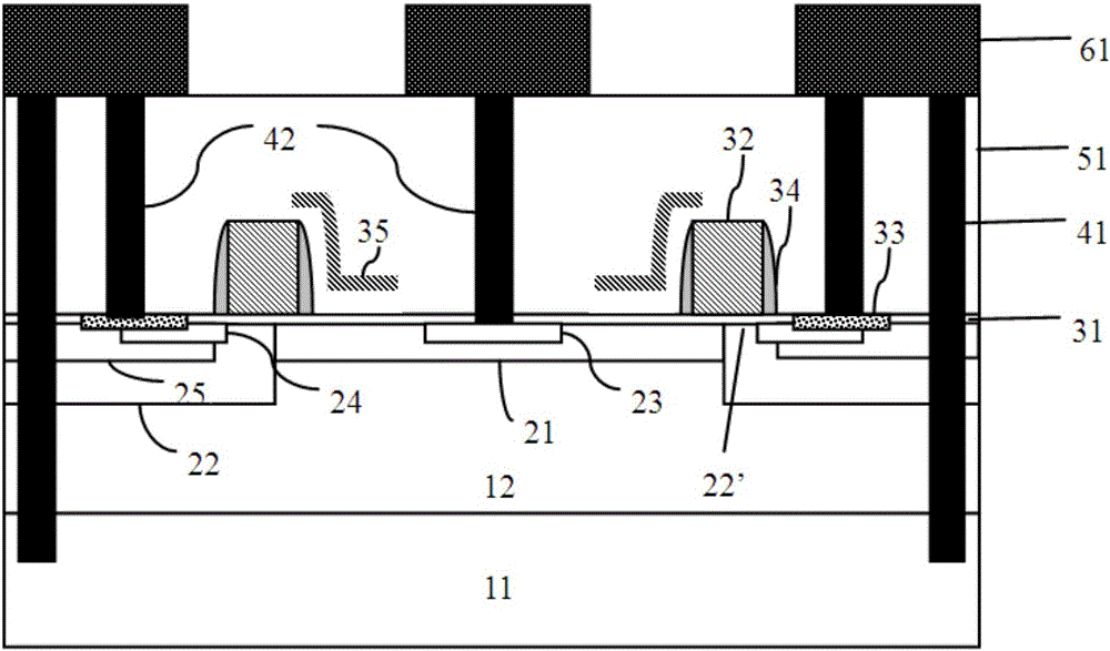
[0036] like figure 1 As shown, an LDMOS device structure includes a metal connection layer 41. The metal connection layer 41 connects the LDMOS device source 24 from the surface to the substrate 11. The material of the metal connection layer 41 is tungsten or copper, and Ti / TiN is used as the contact layer and the blocking layer, the channel is a concentration gradient channel, the channel is a P-type channel, the concentration of the channel near the source 24 is high, and the gate length of the LDMOS device is 90-250nm.

[0037] A method for fabricating an LDMOS device structure, comprising the following steps:

[0038] Step 1, gate oxide and gate deposition;

[0039] Step 2, after gate etc...


PUM

PropertyMeasurementUnit
thicknessaaaaaaaaaa
cover factoraaaaaaaaaa

Abstract

The invention discloses an LDMOS device structure which comprises a metal connection layer. Through the metal connection layer, an LDMOS device source electrode is connected with a substrate from the surface. An LDMOS device channel is a concentration gradient channel. The invention further discloses the manufacture method of the device structure. According to the invention, after polysilicon etching, a medium layer of high step coverage rate is deposited and is used as an injection barrier layer; the problem of photoetching alignment accuracy is solved; self-alignment injection of gate length below 0.25um is realized; through the metal connection layer, the source electrode is connected with the substrate from the surface; after a device is formed, a metal connection layer process is carried out, and gate length below 0.25um is realized; and the manufacture yield and the uniformity can be ensured.

Description

technical field [0001] The invention relates to an LDMOS device structure and a manufacturing method, belonging to the field of semiconductor integrated circuit manufacturing. Background technique [0002] RFLDMOS is an improved N-channel MOSFET designed for RF power amplifiers, with a lateral communication structure, and the drain, source and gate are all on the chip surface. The source is generally connected to the bottom of the substrate by a channel with high impurity concentration in the body and grounded, and there is a low-concentration N-type drift region between the channel and the drain. LDMOS adopts double diffusion technology, and boron and phosphorus are diffused twice in the same photolithography window successively. The channel length can be accurately determined by the difference in the lateral junction depth of the two impurity diffusions. The channel length L can be made very small and is not limited by the photolithography precision. Since LDMOS is easy ...

Claims


Application Information

Patent Timeline
Patent Type & Authority Applications(China)
IPC IPC(8): H01L29/78H01L29/417H01L29/10H01L29/36H01L21/336
CPCH01L29/78H01L29/7816H01L29/1045H01L29/36H01L29/4175H01L29/66689
Inventor 彭虎张耀辉莫海锋
Owner KUNSHAN HUATAI ELECTRONICS TECH CO LTD
Why Eureka
Try Eureka