
Graphene light detector based on metamaterial structure

A photodetector and graphene technology, applied in the direction of semiconductor devices, sustainable manufacturing/processing, electrical components, etc., can solve the problems of high electromagnetic loss, modulation speed limitation, and equivalent capacitance increase, and achieve high modulation speed, Easy integration and small equivalent capacitance

Active Publication Date: 2016-08-17
XIAMEN UNIV
View PDF4 Cites 2 Cited by
  • Summary
  • Abstract
  • Description
  • Claims
  • Application Information

AI Technical Summary

Problems solved by technology

However, the disadvantage of the waveguide structure is that in order to achieve a large modulation depth, the waveguide must be long enough to enhance the interaction between graphene and the light field, which will increase the equivalent capacitance of the waveguide, thereby limiting the modulation speed. At the same time, there will be relatively high electromagnetic losses

Method used


Image

  • Graphene light detector based on metamaterial structure
  • Graphene light detector based on metamaterial structure
  • Graphene light detector based on metamaterial structure

Examples


Embodiment Construction

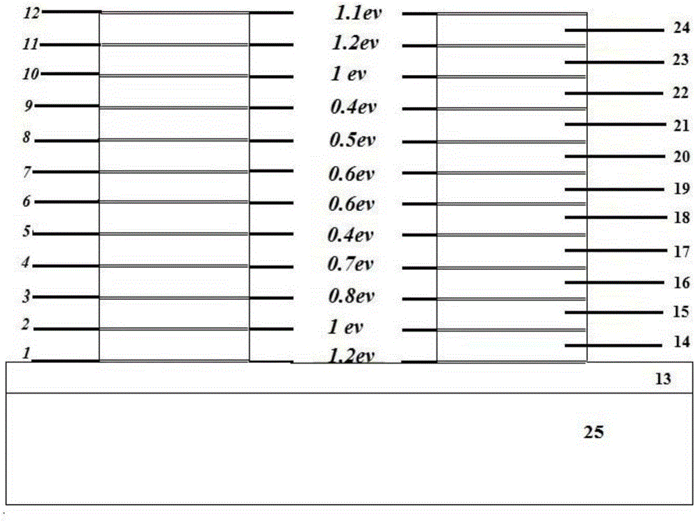
[0025] Choose a single-sided polished silicon wafer as the substrate, evaporate 150nm gold on the substrate by electron beam evaporation, and deposit 180nm Si by radio frequency magnetron sputtering 3 N 4 On Au, then use chemical deposition method to let graphene grow on Si 3 N 4 On, and then use the method of plasma chemical deposition, the 180nm Si 3 N 4 formed on graphene. Repeated 12 times in turn.

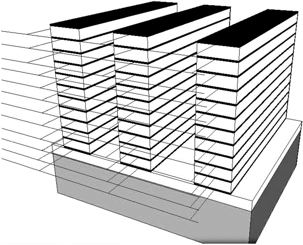
[0026] What the present invention adopts is metal layer-medium layer-graphene layer-medium layer-graphene layer-medium layer-graphene layer-medium layer-graphene layer-medium layer-graphene layer-medium layer-graphene layer- Dielectric layer - graphene layer - dielectric layer - graphene layer - dielectric layer - graphene layer - dielectric layer - graphene layer - dielectric layer - graphene layer - dielectric layer - graphene layer its composition see figure 1 , figure 2 .

[0027] exist figure 1 and 2 Among them, marks 1-12 are single-atom graphene layers, and ...


PUM

PropertyMeasurementUnit
lengthaaaaaaaaaa
widthaaaaaaaaaa
thicknessaaaaaaaaaa

Abstract

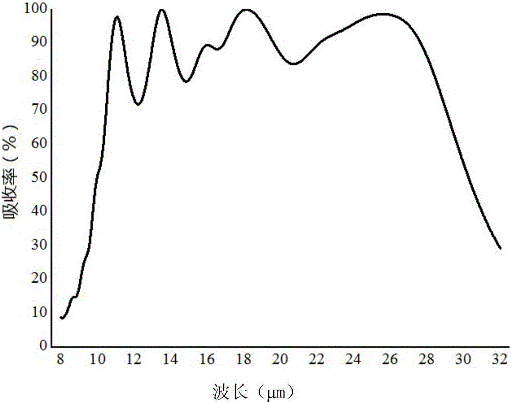
The invention provides a graphene light detector based on a metamaterial structure and relates to a light detector. The graphene light detector based on the metamaterial structure can achieve ultra-wide-band absorption. The graphene light detector is of a laminated structure and includes a metal layer, a medium layer, a graphene layer, a medium layer, a graphene layer, a medium layer, a graphene layer, a medium layer, a graphene layer, a medium layer, a graphene layer, a medium layer, a graphene layer, a medium layer, a graphene layer, a medium layer, a graphene layer, a medium layer, a graphene layer, a medium layer, a graphene layer, a medium layer, a graphene layer, a medium layer and a graphene layer in sequence from top to bottom in the vertical direction. In the horizontal direction, the graphene layers and the medium layers are grid-shaped strips, the strips are arranged cyclically, and bias voltage is added for each graphene layer and used for changing the refractive index of graphene so as to dynamically regulate and control the spatial refractive index of each graphene layer and further adjust the spatial absorptivity of the whole structure.

Description

technical field [0001] The invention relates to a photodetector, in particular to a graphene photodetector based on a metamaterial structure. Background technique [0002] Light absorption is an important link in the study of photodetectors and solar photovoltaic effects. Broadband optical detectors are widely used in many important fields, including infrared imaging, remote sensing, environmental monitoring, astronomical detection, spectral analysis, etc. Especially in the field of infrared imaging, in order to realize multi-color infrared imaging in the true sense, the detector must be able to simultaneously detect infrared radiation of different bands such as short-wave infrared (1-3mm), medium-wave infrared (3-5mm), long-wave infrared ( 8~14mm), very long wave infrared (>14mm), and even terahertz wave (30~3000mm) radiation, which is quite challenging. At present, in order to achieve multi-color infrared imaging to a certain extent, it is necessary to integrate multi...

Claims


Application Information

Patent Timeline
Patent Type & Authority Applications(China)
IPC IPC(8): H01L31/028H01L31/09H01L31/18
CPCH01L31/028H01L31/09H01L31/1804Y02P70/50
Inventor 朱锦锋李嘉晔刘海柳清伙
Owner XIAMEN UNIV
Learn More