Growth method of type-n monocrystalline silicon
A growth method and technology of single crystal silicon, which are applied to the growth of single crystal silicon for n-type semiconductors and the growth of single crystal silicon with narrow resistivity fluctuations, which can solve the problem of different segregation coefficients and double doping resistivity deviation from the initial value. , the different degree of volatilization of doping elements, etc.
- Summary
- Abstract
- Description
- Claims
- Application Information
AI Technical Summary
Problems solved by technology
Method used
Image

Examples
Embodiment 1
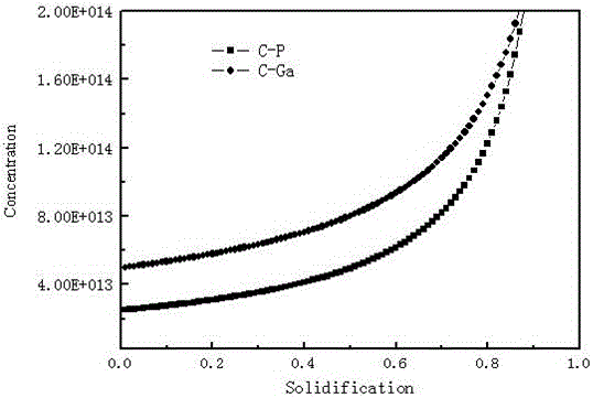
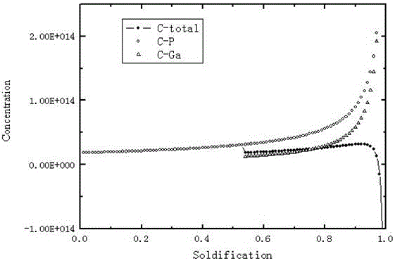
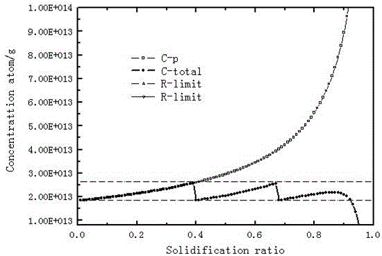
[0061] 8-inch n-type single crystal silicon rods in direction were grown by CZ method. Add 120kg of polysilicon raw material and phosphorus into the quartz crucible, and the resistivity target value is 60-100Ω, which is the highest resistivity R si-max 100Ω, minimum resistivity R si-min is 60Ω. According to formula (1) from the highest resistivity R si-max The initial concentration of phosphorus is obtained as 5.9×10 13 atom / g, at the same time by the lowest resistivity R si-min It is calculated that the solidification rate is 0.54 at the point where the secondary doping element is added.
[0062] In a specific implementation, under the protection of an inert gas, the adsorbed oxygen in the raw material is removed. Turn on the heater and gradually raise the temperature to above 1420°C to completely melt the raw materials. According to the conventional crystal growth parameters, seeding, shouldering, shoulder turning, and entering the equal-diameter stage are carried out...
Embodiment 2
[0065] 8-inch n-type single crystal silicon rods in direction were grown by CZ method. Add 120kg of polysilicon raw material and phosphorus into the quartz crucible, and the resistivity target value is 70-100Ω, that is, the highest resistivity R si-max 100Ω, minimum resistivity R si-min is 70Ω. According to formula (1) from the highest resistivity R si-max The initial concentration of phosphorus is obtained as 5.9×10 13 atom / g, at the same time by the lowest resistivity R si-min It is calculated that the secondary doping elements need to be added twice, and the solidification rates at the addition points are 0.40 and 0.68, respectively.
[0066] In a specific implementation, under the protection of an inert gas, the adsorbed oxygen in the raw material is removed. Turn on the heater and gradually raise the temperature to above 1420°C to completely melt the raw materials. According to the conventional crystal growth parameters, seeding, shouldering, shoulder turning, and ...
Embodiment 3
[0070] 8-inch n-type single crystal silicon rods in direction were grown by CZ method. Add 120kg of polysilicon raw material and phosphorus into the quartz crucible, and the resistivity target value is 80-100Ω, which is the highest resistivity R si-max 100Ω, minimum resistivity R si-min is 80Ω. According to formula (1) from the highest resistivity R si-max The initial concentration of phosphorus is obtained as 5.9×10 13 atom / g, at the same time by the lowest resistivity R si-min It is calculated that the secondary doping elements need to be added four times, and the curing rates at the addition points are 0.25, 0.47, 0.63 and 0.78, respectively.
[0071] In a specific implementation, under the protection of an inert gas, the adsorbed oxygen in the raw material is removed. Turn on the heater and gradually raise the temperature to above 1420°C to completely melt the raw materials. According to the conventional crystal growth parameters, seeding, shouldering, shoulder turn...
PUM
 Abstract
Description
Claims
Application Information
 - R&D
- Intellectual Property
- Life Sciences
- Materials
- Tech Scout
- Unparalleled Data Quality
- Higher Quality Content
- 60% Fewer Hallucinations
Browse by: Latest US Patents, China's latest patents, Technical Efficacy Thesaurus, Application Domain, Technology Topic, Popular Technical Reports.
© 2025 PatSnap. All rights reserved.Legal|Privacy policy|Modern Slavery Act Transparency Statement|Sitemap|About US| Contact US: help@patsnap.com