Optical source assembly structure of flip LED chip integrated package and manufacturing method thereof

A technology of LED chips and light source components, applied in the field of LED light sources, can solve the problems of reduced contact fastness and reliability of chip electrodes, chip displacement, and smaller heat dissipation channel area of ​​the chip, etc., so as to ensure the photoelectric characteristics and reliability, Improve production capacity and shipment rate, maximize the effect of heat dissipation area

Active Publication Date: 2016-08-24
湖南省日晶照明科技有限责任公司
View PDF5 Cites 25 Cited by
  • Summary
  • Abstract
  • Description
  • Claims
  • Application Information

AI Technical Summary

Problems solved by technology

The actual problem encountered is that during the heating and curing process of the patch, the chip is often displaced on the COB due to the difficulty in controlling the amount of paste in the two areas of the P and N electrodes, or the distance between the two areas is too small. , resulting in a short circuit between the P and N electrodes
If the distance between the two glue points is too large, the contact area between the chip and the COB board will be reduced, that is, the heat dissipation channel area of ​​the chip will be reduced, which directly affects the light efficiency and the reliability of the light source driven by high current.
In addition, the flux contained in the solder paste and other materials used in the current LED packaging industry will easily form voids at the connection interface after reflow soldering volatilizes, which will also further reduce the heat dissipation surface of the chip
[0005] In addition, after the flux in the general solder paste volatilizes, brown matter often remains between the LED chip surface and the COB board surface, absorbing part of the light and reducing the light output of the light source; moreover, large voids and residues in the gap Volatile matter such as gas expands when the temperature of the chip is driven by a large current, which eventually leads to a decrease in the contact fastness and reliability of the chip electrode.
At present, conductive paste is applied to the P and N electrodes of each flip-chip on the COB board. The more chips, the more solder joints, the more chances of the above-mentioned disadvantages, and the impact on the quality of the light source. also more serious

Method used


Image

  • Optical source assembly structure of flip LED chip integrated package and manufacturing method thereof
  • Optical source assembly structure of flip LED chip integrated package and manufacturing method thereof
  • Optical source assembly structure of flip LED chip integrated package and manufacturing method thereof

Examples


Embodiment 1

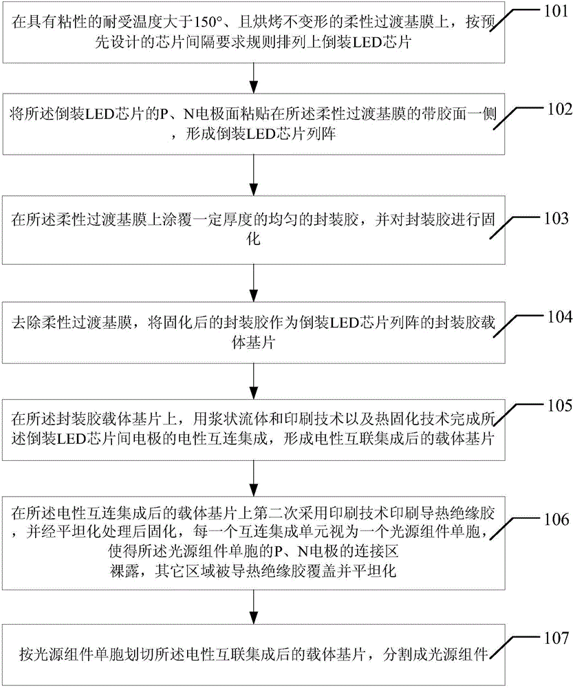
[0047] Such as Figure 2A and Figure 2B As shown, it is a top view and a side view of the light source assembly structure of the flip-chip LED chip integrated package of the present invention, see figure 1 , the manufacturing method of the light source assembly structure described in the present embodiment, comprises the following steps:

[0048] Step 101. Arrange flip-chip LED chips on the sticky flexible transition base film that can withstand a temperature greater than 150° and is not deformed when baked according to the pre-designed chip spacing requirements;

[0049] Step 102, sticking the P and N electrode surfaces of the flip-chip LED chip on the adhesive side of the flexible transition base film to form a flip-chip LED chip array;

[0050] Step 103, coating a certain thickness of uniform encapsulation glue on the flexible transition base film, and curing the encapsulation glue;

[0051] Specifically, by attaching a dam 40 of a certain height around the flip-chip LE...

Embodiment 2

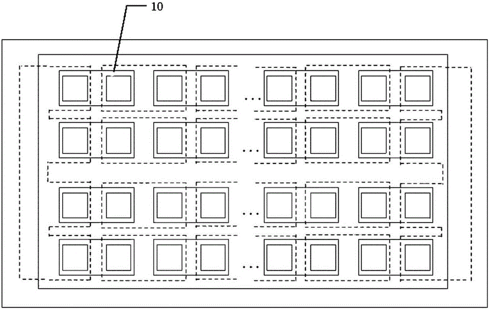
[0066] Such as Figure 2A , Figure 2B As shown, it is a top view and a side view of the light source assembly structure of the flip-chip LED chip integrated package of the present invention. The carrier substrate 61 after permanent interconnection and integration, and the unit cell of the light source module after the second printing of heat-conducting insulating glue;

[0067] Flip-chip LED chips 10, encapsulation glue carrier substrates of flip-chip LED chip arrays, carrier substrates after electrical interconnection integration, and light source component cells after secondary printing of heat-conducting insulating glue; wherein,

[0068] The encapsulation adhesive carrier substrate of the flip-chip LED chip array is on a flexible transition base film with a viscosity that can withstand a temperature greater than 150° and is not deformed when baked, and is flip-chip arranged regularly according to the pre-designed chip spacing requirements. LED chips; paste the P electro...

Embodiment 3

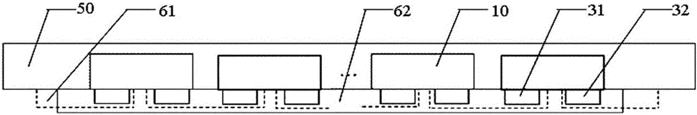
[0075] The following provides an application example of the manufacturing method of the light source component structure of the flip-chip LED chip integrated package of the present invention, see image 3 ,include:

[0076] Step 201. Arrange a plurality of flip-chip LED chips 10 on the flexible transition base film (conversion base film) 20 according to the designed chip spacing requirements, and paste the P electrodes 31 and N electrodes 32 of the flip-chip LED chips 10 on the flexible transition base film (conversion base film) 20. One side of the adhesive surface of the transition base film 20 forms an array of flip-chip LED chips, see Figure 4 .

[0077]Wherein, the flip-chip LED chip 10 is a chip sorted according to the excitation wavelength of the phosphor powder. The flip-chip LED chips are arranged equidistantly on the flexible transition base film 20 according to the design requirements, and the electrode surface of the flip-chip LED chip 10 is adhered to the flexi...


PUM


Abstract

The invention discloses an optical source assembly structure of flip LED chip integrated package and a manufacturing method thereof. The method comprises the steps of arranging flip LED chips on a flexible transition base film to form a chip array; coating the base film uniformly with packaging glue to a certain thickness, and curing the packaging glue; removing the flexible transition base film, and using the cured packaging glue as a carrier substrate of the chip array; completing the electrical interconnect integration of electrodes among the chips on the packaging glue carrier substrate; printing and curing thermally conductive and insulation glue on the carrier substrate after electrical interconnect integration, to form various optical source assembly unit cells; and obtaining a separated optical source assembly in accordance with the various optical source assembly unit cells. The optical source assembly is bonded and assembled with a thermally conductive substrate to achieve electrical connection with an external circuit to be combined into an optical source. The method is free from the form of isolated chip interconnect integrated package on a COB board in the current packaging industry, eliminates the process steps of surface mounting and crystal curing and the like on the COB board, and simplifies the manufacturing process.

Description

technical field [0001] The present invention relates to the technical field of LED light sources, in particular to a structure of a light source component integrated and packaged with flip-chip LED chips and a manufacturing method thereof. Background technique [0002] As a new type of industrial product, LED (Light Emitting Diode) has the characteristics of low working voltage, small working current, good shock resistance and shock resistance, high reliability, and long life. more and more common. In recent years, research efforts in the field of LEDs have become more and more intensive, and light sources composed of LED chips have also become a key research topic. Among them, further improving the manufacturing efficiency of the light source, reducing the manufacturing cost, and improving the luminous efficiency and reliability have become important research contents. [0003] LED flip chip is a new generation of product that has been widely recognized by the LED industr...

Claims


Application Information

Patent Timeline
Patent Type & Authority Applications(China)
IPC IPC(8): H01L33/52H01L33/62
CPCH01L33/52H01L33/62H01L2224/04105H01L2224/18H01L2224/24137H01L2224/96H01L2933/005H01L2933/0066
Inventor 王良臣汪延明苗振林张雪亮谈健
Owner 湖南省日晶照明科技有限责任公司
Why Eureka
Try Eureka