Nanometer scale flexible transparent circuit and preparation process thereof

A preparation process, nano-level technology, applied in the direction of printed circuit manufacturing, printed circuits, printed circuit components, etc., can solve the requirements that the display screen cannot be adapted to the sensitivity and accuracy, the sensitivity and accuracy of the display screen is not high, and the position of the surface changes. Insufficient sensitivity, etc., to achieve the effect of small distance, small width and low cost

Active Publication Date: 2016-08-24
SHANGHAI JIAO TONG UNIV
View PDF6 Cites 14 Cited by
  • Summary
  • Abstract
  • Description
  • Claims
  • Application Information

AI Technical Summary

Problems solved by technology

Due to the wide width of the wires and the large distance between adjacent wires, the current transparent grid circuit of the flexible electrode is not sensitive enough to the change of the surface position, and cannot meet the sensitive and accurate requirements of the display screen.
[0003] Chinese patent 201110091338.9 discloses a bendable flexible transparent electronic circuit and its preparation method, which can be used to print the circuit on the flexible circuit board and maintain the bendable and transpare...

Method used


Image

  • Nanometer scale flexible transparent circuit and preparation process thereof
  • Nanometer scale flexible transparent circuit and preparation process thereof
  • Nanometer scale flexible transparent circuit and preparation process thereof

Examples


Embodiment 1

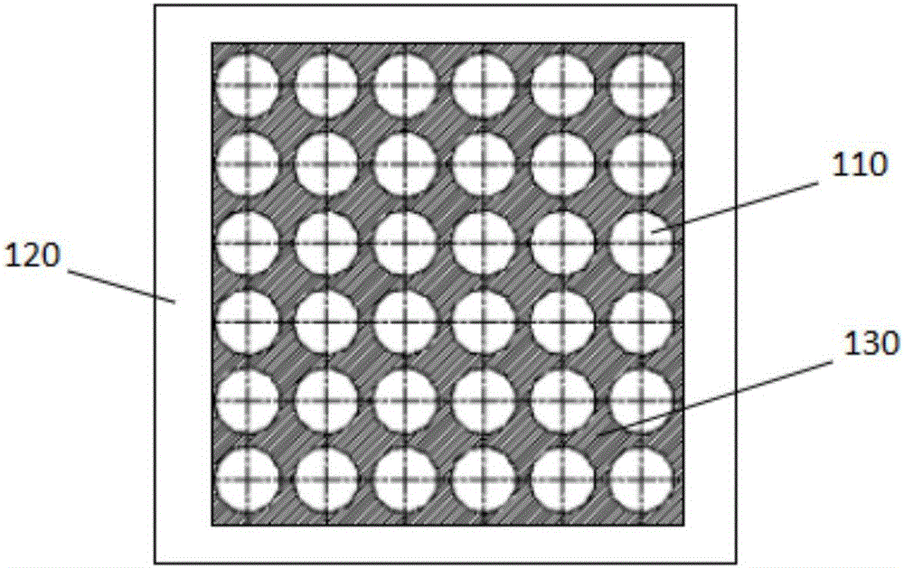
[0032] A nanoscale flexible transparent circuit, its structure is as figure 1 As shown, it is composed of PET base 120 , UV photocurable resin 110 and nano-silver paste 130 , UV photo-curable resin layer 110 is laid on PET base layer 120 , and nano-silver paste 130 fills the structural gap with resin layer 110 . The structure of the UV curable resin 110 adopts a cylindrical structure, the diameter of the cylinder is 700nm, the distance between the centers of adjacent cylinders is 800nm, and the height of the cylinder is 200nm.

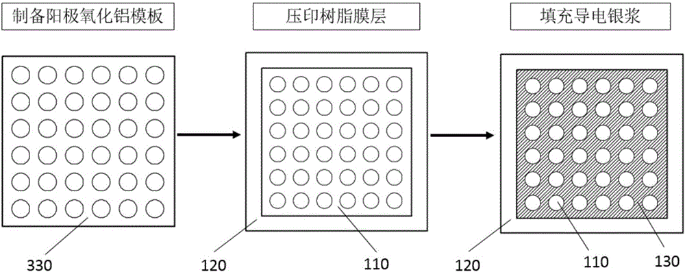
[0033] image 3 and Figure 4 They are respectively the process flow diagram and the schematic diagram of the anodized aluminum template production process of the present invention. The aluminum or aluminum alloy plate 330 is used as the anode, and the carbon rod 310 is used as the cathode. Aluminum oxide film is formed on the surface of 330, so that the nanoporous anodized aluminum oxide film and aluminum without anodic oxidation form a roll-to-roll...

Embodiment 2

[0037] A nanoscale flexible transparent circuit, its structure is as figure 1 As shown, the difference from Embodiment 1 is that in this embodiment, a layer of UV curable resin layer 110 is laid on the surface of the PET layer 120 by a flat pressing process, and finally the conductive silver paste 130 is filled in the gaps of the resin structure.

Embodiment 3

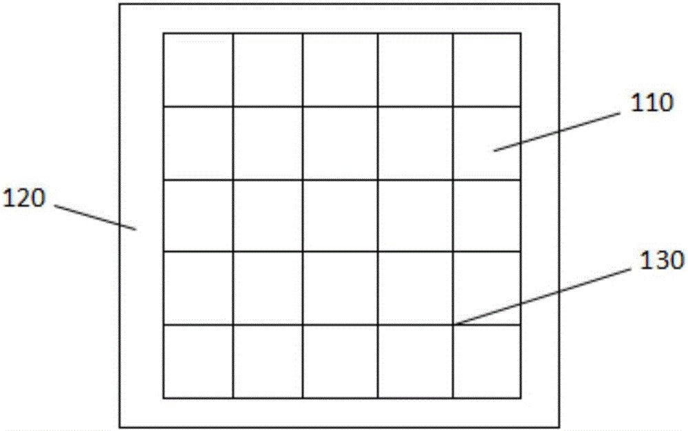
[0039] A nanoscale flexible transparent circuit, its structure is as figure 2 As shown, it is roughly the same as in Example 1, except that the resin structure in this embodiment adopts a quadrangular prism structure, the bottom side length of the quadrangular prism is 400nm, the center-to-center distance between adjacent quadrangular prisms is 450nm, and the height of the quadrangular prism is 500nm.


PUM

PropertyMeasurementUnit
Particle sizeaaaaaaaaaa
Heightaaaaaaaaaa
Groove widthaaaaaaaaaa

Abstract

The invention relates to a nanometer scale flexible transparent circuit and a preparation method thereof. The nanometer scale flexible transparent circuit is composed of a PET substrate, a UV light-cured resin and nanoscale silver paste; the UV light-cured resin is laid on the PET substrate; and the nanoscale silver paste is filled in a structure gap of the UV light-cured resin. Compared with the prior art, the nanometer scale flexible transparent circuit provided by the invention is simple in structure and reasonable in design, a nano rolled template is manufactured by adopting a processing technology of anodized aluminum, so that the preparation efficiency of a resin structure is high, the cost is low, and the limit that traditional machining cannot produce a nanostructure can be broken through; besides, the nanostructure in an array arrangement can be quickly prepared, and the commercial demands of being low in cost, fast, large in area, high in resolution and high in throughput can be satisfied.

Description

technical field [0001] The invention belongs to the field of display technology, and in particular relates to a nanoscale flexible transparent circuit and a preparation process thereof. Background technique [0002] Flexible displays made of flexible materials make up for the shortcomings of traditional rigid displays that are not deformable and not easy to carry, and have become a major development direction in the field of display technology. The flexible display realizes the function of being foldable and easy to carry. It can be "rolled" up and put in a bag, or it can be folded and stuffed into a pocket. At the same time, flexible displays can also be embedded in watches, glasses and other items to become everyday wearable devices. Due to the wide width of the wires and the large distance between adjacent wires, the current transparent grid circuit of the flexible electrode is not sensitive enough to the change of the position of the surface, and cannot meet the sensiti...

Claims


Application Information

Patent Timeline
IPC IPC(8): H05K1/09H05K3/12
CPCH05K1/097H05K3/1258H05K2203/0522H05K2203/0545
Inventor 易培云张成鹏朱宇文彭林法来新民
Owner SHANGHAI JIAO TONG UNIV
Why Eureka
Try Eureka