A method for growing light-emitting diode epitaxial wafers

A technology of light-emitting diodes and growth methods, which is applied in the field of growth of light-emitting diode epitaxial wafers, can solve the problems of low luminous efficiency of LEDs, and achieve the effects of improving luminous efficiency, improving crystal quality, and reducing defects

Active Publication Date: 2018-04-24
HC SEMITEK SUZHOU
View PDF8 Cites 0 Cited by
  • Summary
  • Abstract
  • Description
  • Claims
  • Application Information

AI Technical Summary

Problems solved by technology

[0006] In order to solve the problem of low luminous efficiency of LEDs in the prior art, an embodiment of the present invention provides a method for growing a light emitting diode epitaxial wafer

Method used


Image

  • A method for growing light-emitting diode epitaxial wafers

Examples


Embodiment

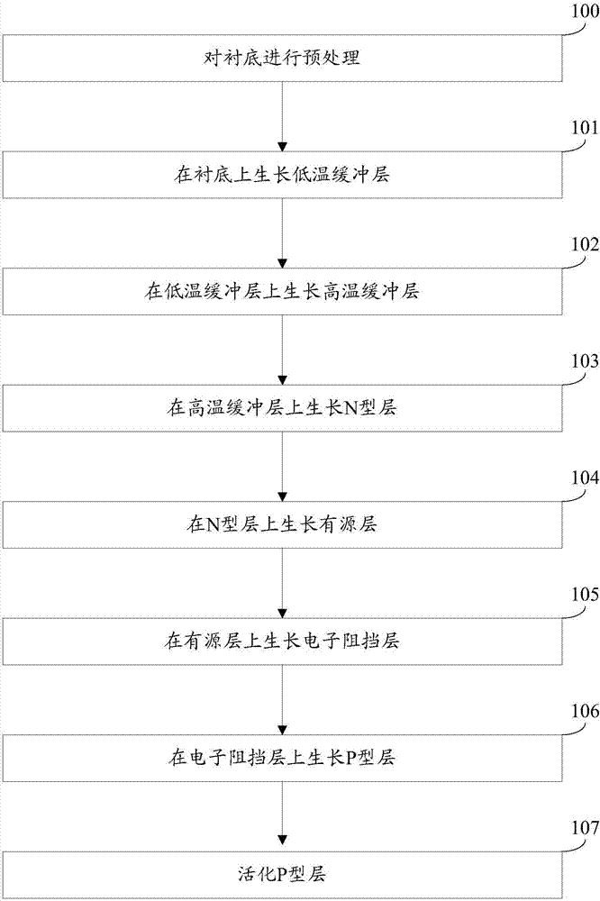
[0026] An embodiment of the present invention provides a method for growing a light-emitting diode epitaxial wafer, see figure 1 , the growth method includes:

[0027] Step 100: Perform pretreatment on the substrate.

[0028] In this embodiment, the substrate is a sapphire substrate.

[0029] Specifically, this step 100 may include:

[0030] Under a hydrogen atmosphere, treat the substrate at a high temperature for 5 min to 6 min. Wherein, the temperature of the reaction chamber is 1000° C. to 1100° C., and the pressure of the reaction chamber is controlled at 200 torr to 500 torr.

[0031] In this embodiment, a Veeco K465i or C4 metal organic compound chemical vapor deposition (MetalOrganic Chemical Vapor Deposition, MOCVD) equipment is used to realize the LED growth method. Using high-purity hydrogen (H 2 ), high-purity nitrogen (N 2 ) or high purity H 2 and high purity N 2 The mixed gas as the carrier gas, high-purity NH 3 As the N source, trimethylgallium (TMGa) a...


PUM


Abstract

The invention discloses a growth method for a light-emitting diode epitaxial wafer, and belongs to the technical field of semiconductors. The method comprises the step: sequentially growing a low-temperature buffering layer, a high-temperature buffering layer, an N-type layer, an active layer, an electronic blocking layer and a P-type layer on a substrate. The active layer comprises a first sub-layer and a second sub-layer, and the growth atmospheres of a quantum well layer in the first sub-layer, a quantum barrier layer in the first sub-layer, a quantum well layer in the second sub-layer and a quantum barrier layer in the second sub-layer are sequentially N2 and H2 mixed gas, pure H2, pure N2, and N2 and H2 mixed gas. The quantum well layer in the first sub-layer employs a variable pressure and variable temperature growth mode, and the quantum barrier layer in the first sub-layer employs a high-pressure and high-temperature growth mode. The quantum well layer in the second sub-layer employs a low-pressure and low-temperature growth mode, and the quantum barrier layer in the second sub-layer employs a variable pressure growth mode. The quantum barrier layer in the first sub-layer employs trimethyl gallium as a gallium source. The method improves the light-emitting efficiency.

Description

technical field [0001] The invention relates to the technical field of semiconductors, in particular to a method for growing a light-emitting diode epitaxial wafer. Background technique [0002] Light Emitting Diode (LED for short) is a semiconductor electronic component that can emit light. As a new type of high-efficiency, environmentally friendly and green solid-state lighting source, LEDs are rapidly and widely used in fields such as traffic lights, interior and exterior lights of automobiles, urban landscape lighting, and mobile phone backlights. [0003] The existing LED epitaxial wafer growth method is to sequentially grow a low-temperature buffer layer, a high-temperature buffer layer, an N-type layer, an active layer, and a P-type layer on a substrate, wherein the active layer includes alternately stacked quantum well layers and quantum barriers. layer, quantum well layer and quantum barrier layer growth conditions are kept unchanged. [0004] In the process of re...

Claims


Application Information

Patent Timeline
Patent Type & Authority Patents(China)
IPC IPC(8): H01L33/00
CPCH01L33/007
Inventor 姚振从颖胡加辉
Owner HC SEMITEK SUZHOU
Why Eureka
Try Eureka