Single-layer meta-material surface structure capable of realizing angle-selective filtering through filtering frequency change
A technology of frequency selection and surface structure, applied in electrical components, antennas, etc., can solve problems such as heavy workload, reduced antenna work efficiency, complex structure, etc., to achieve the effect of simplifying structure, easy to optimize design, and less structural parameters
- Summary
- Abstract
- Description
- Claims
- Application Information
AI Technical Summary
Problems solved by technology
Method used
Image
Examples
Embodiment 1
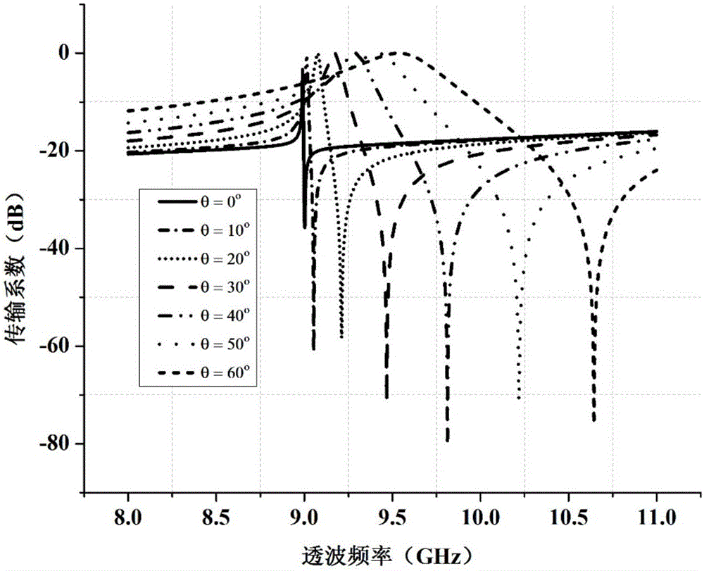
[0034] Embodiment 1, a metamaterial surface structure with a wave-transmitting frequency range of 8.99 GHz to 9.54 GHz.
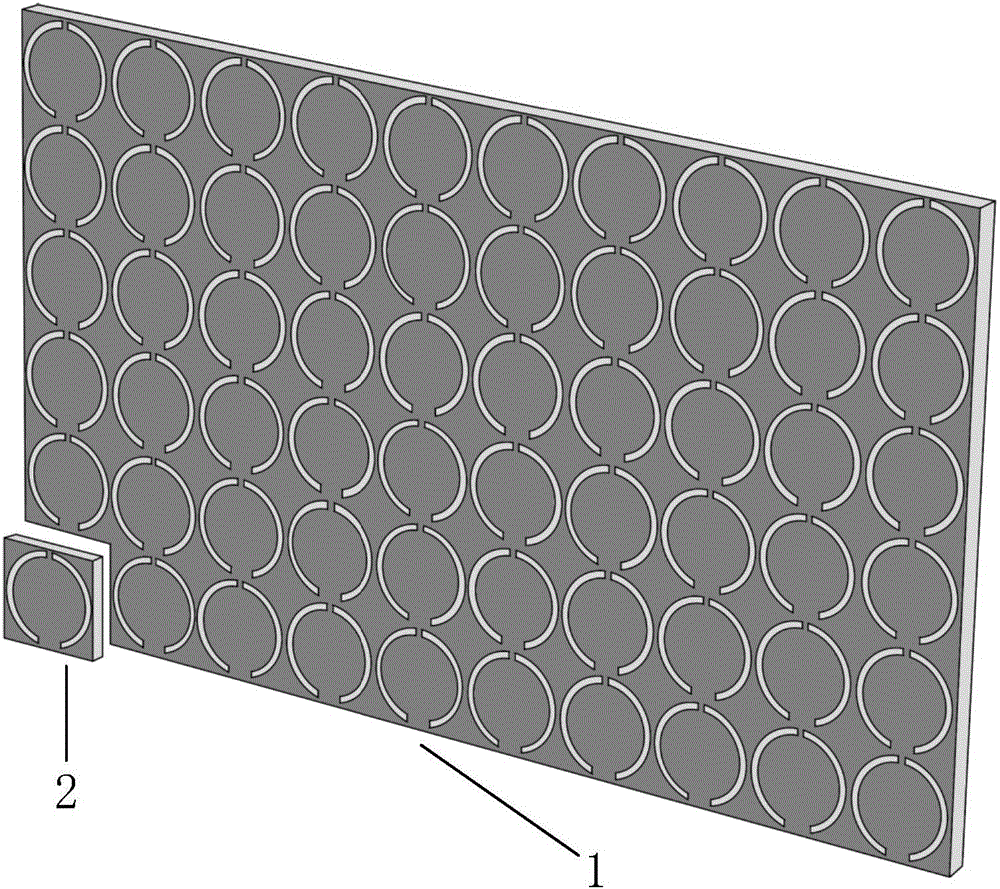
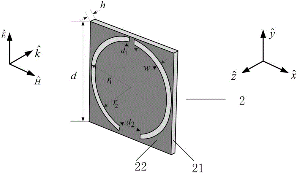
[0035] Each single-layer metasurface gap unit 2 in this example includes a dielectric substrate 21 and a metal patch 22 .
[0036] The dielectric substrate 21 adopts a square organic polymer substrate with a side length d of 8 mm, a thickness h of 0.5 mm, and a dielectric constant of 2.65;
[0037] The metal patch 22 adopts a metal copper material with a side length d of 8 mm, on which an annular gap with upper and lower asymmetrical double openings is etched, and the upper opening width of the annular gap is d 1 0.1mm, the lower opening d of the annular gap 2 0.3mm, the outer diameter r of the annular gap 1 is 3.9mm, the inner diameter r of the annular gap 2 is 3.8mm, and the width w of the annular gap is 0.1mm.
[0038] Each single-layer metasurface slit unit 2 is closely arranged on the single-layer metamaterial surface 1 in the form of M×N matrix, and...
Embodiment 2
[0039] Embodiment 2, a metamaterial surface structure with a wave-transmitting frequency range of 12.08 GHz to 12.4 GHz.
[0040] The structure of this example is the same as that of Example 1, and its parameters are changed as follows:
[0041] The dielectric substrate 21 adopts a square organic polymer substrate with a side length d of 8 mm, a thickness h of 0.6 mm, and a dielectric constant of 3.27;
[0042] The metal patch 22 adopts a metal copper material with a side length d of 8 mm, and the opening width d on the annular gap is 1 1mm, opening d under the annular gap 2 is 2.5mm, the outer diameter of the annular gap r 1 is 3.5mm, the inner diameter of the annular gap r 2 is 3.1mm, and the width w of the annular gap is 0.4mm.
[0043] This example can realize that the wave transmission angle θ changes from 0° to 60° with the wave transmission frequency of 12.08GHz to 12.4GHz.
Embodiment 3
[0044] Embodiment 3, a metamaterial surface structure with a wave-transmitting frequency range of 15.51 GHz to 16.26 GHz.
[0045] The structure of this example is the same as that of Example 1, and its parameters are changed as follows:
[0046] The dielectric substrate 21 adopts a square organic polymer substrate with a side length d of 8 mm, a thickness h of 0.8 mm, and a dielectric constant of 4.4;
[0047] The metal patch 22 adopts a metal copper material with a side length d of 8 mm, and the opening width d on the annular gap is 1 3.7mm, opening d under the annular gap 2 is 4mm, the outer diameter r of the annular gap 1 is 3.9mm, the inner diameter r of the annular gap 2 is 2mm, and the width w of the annular gap is 1.9mm.
[0048] This example can realize the change of the wave transmission angle θ from 0° to 60° with the wave transmission frequency of 15.51 GHz to 16.26 GHz.
[0049] The technical effects of the present invention will be further described in detai...
PUM
 Abstract
Description
Claims
Application Information


