Nonvolatile resistive random access memory device and preparation method thereof

A resistive memory, non-volatile technology used in the field of microelectronics

Active Publication Date: 2016-10-05
INST OF MICROELECTRONICS CHINESE ACAD OF SCI
View PDF5 Cites 20 Cited by
  • Summary
  • Abstract
  • Description
  • Claims
  • Application Information

AI Technical Summary

Problems solved by technology

[0007] From the above, the purpose of the present invention is to overcome the above-mentioned technical difficulties, the shortcomings of the resistive variable memory based on the formation and fracture principle of metal conductive filaments, and to provide a method that can control the formation position of conductive filaments and control the conductive filaments. A new device structure and its manufacturing method to reduce the discreteness of the electrical parameters of the resistive variable memory through the formation process, which improves the performance and reliability of the device

Method used


Image

  • Nonvolatile resistive random access memory device and preparation method thereof
  • Nonvolatile resistive random access memory device and preparation method thereof
  • Nonvolatile resistive random access memory device and preparation method thereof

Examples


Embodiment Construction

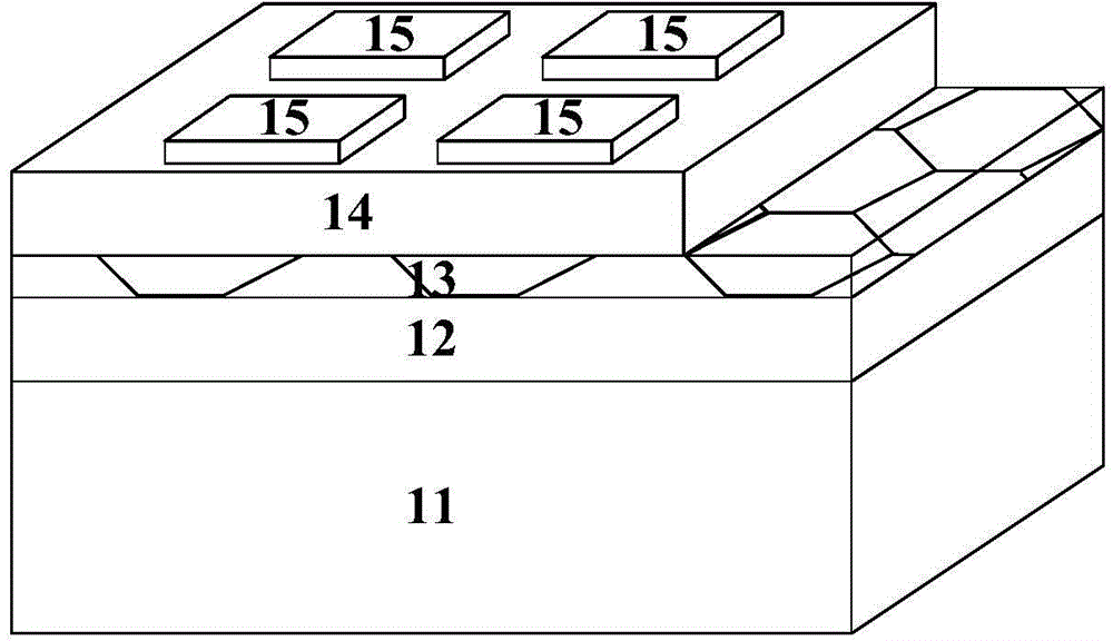
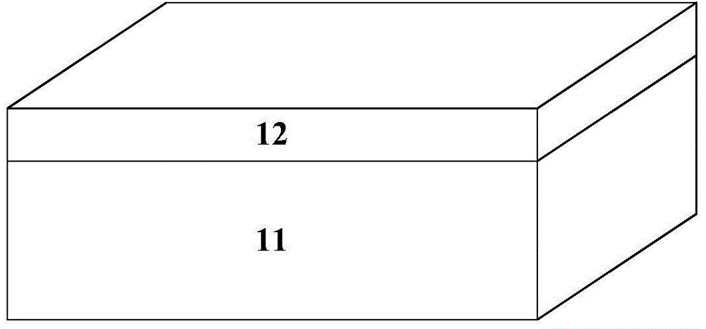
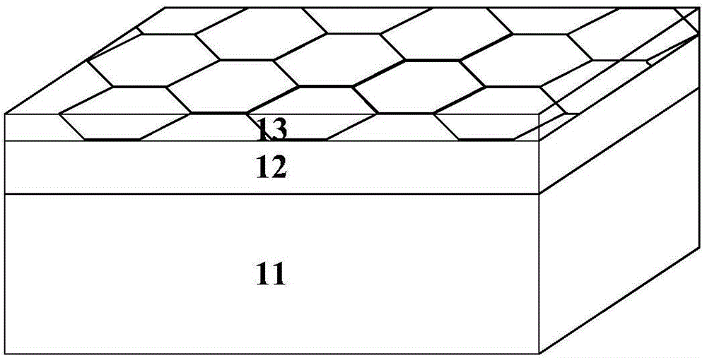
[0030]The features and technical effects of the technical solution of the present invention will be described in detail below with reference to the accompanying drawings and in conjunction with schematic embodiments, which discloses that a graphene intercalation structure containing nanopores is added between the easily oxidizable metal electrode and the resistive function layer. A non-volatile resistive memory device and a manufacturing method thereof. It should be pointed out that similar reference numerals represent similar structures, and the terms "first", "second", "upper", "lower" and the like used in this application can be used to modify various device structures or manufacturing processes . These modifications do not imply spatial, sequential or hierarchical relationships of the modified device structures or fabrication processes unless specifically stated.

[0031] Such as figure 1 Shown is a schematic diagram of a resistive switching memory device according to th...


PUM

PropertyMeasurementUnit
diameteraaaaaaaaaa
thicknessaaaaaaaaaa
thicknessaaaaaaaaaa

Abstract

A nonvolatile resistive random access memory device comprises an inert metal electrode, a resistive function layer and an oxidation-prone metal electrode. The nonvolatile resistive random access memory device is characterized in that a grapheme barrier layer containing a plurality of nano-pores is inserted between the oxidation-prone metal electrode and the resistive function layer, so that metal ions formed after the metal oxidation of the oxidation-prone metal electrode in a device programming process are controlled to enter the resistive function layer only through the positions of the plurality of nano-pores. According to the invention, the grapheme insertion layer structure containing the nano-pores is added between the oxidation-prone metal electrode and the resistive function layer, the diffusion of the metal ions is blocked, and the metal ions formed by the oxidation-prone metal electrode in the device programming process are enabled to enter the resistive function layer only through the positions of the plurality of nano-pores, so that the growing positions of conductive filaments are controlled.

Description

technical field [0001] The invention belongs to the technical field of microelectronics, and in particular relates to a resistive variable memory unit structure and a manufacturing method based on nanoporous graphene intercalation that can control the growth position of conductive filaments. Background technique [0002] With the demand for large-capacity and low-power storage in multimedia applications and mobile communications, the market share of non-volatile memory, especially flash memory, has become larger and larger, and it has gradually become a very important memory. . The main feature of non-volatile memory is that it can save the stored information for a long time without power on. It not only has the characteristics of read-only memory, but also has a high access speed. [0003] The non-volatile memory currently on the market is mainly flash memory, but flash memory devices have excessive operating voltage, slow operating speed, insufficient durability, and shor...

Claims


Application Information

Patent Timeline
Patent Type & Authority Applications(China)
IPC IPC(8): H01L45/00
CPCH10N70/245H10N70/8416H10N70/826H10N70/021H10N70/8825H10N70/841H10N70/8828H10N70/8833
Inventor 刘琦刘明孙海涛吕杭炳龙世兵瑞塔姆·白纳吉张康玮
Owner INST OF MICROELECTRONICS CHINESE ACAD OF SCI
Why Eureka
Try Eureka