Light source packaging structure, and positioning and coupling method thereof

A packaging structure and grating coupler technology, applied in the coupling of optical waveguides, light guides, optics, etc., can solve the problems of inability to produce high-power light sources, low yield, and chip heat dissipation, and achieve optical passive alignment, Improved service life and compact package structure

Active Publication Date: 2016-10-12
GUANGXUN SCI & TECH WUHAN
View PDF4 Cites 43 Cited by
  • Summary
  • Abstract
  • Description
  • Claims
  • Application Information

AI Technical Summary

Problems solved by technology

With this package structure, the TO package size of the external light source is relatively large, and generally there is no cooling design, and the heat dissipation of the chip is affected. It is not suitable for high-power laser chips and cannot be used to make high-power light sources; the cat's eye angle of the polarization-maintaining fiber at the end FA must be controlled. At + / -5 degrees, the operation is more difficult, the yield is low, and the cost is high

Method used


Image

  • Light source packaging structure, and positioning and coupling method thereof
  • Light source packaging structure, and positioning and coupling method thereof
  • Light source packaging structure, and positioning and coupling method thereof

Examples


Embodiment Construction

[0040] The present invention will be described in detail below in conjunction with the accompanying drawings.

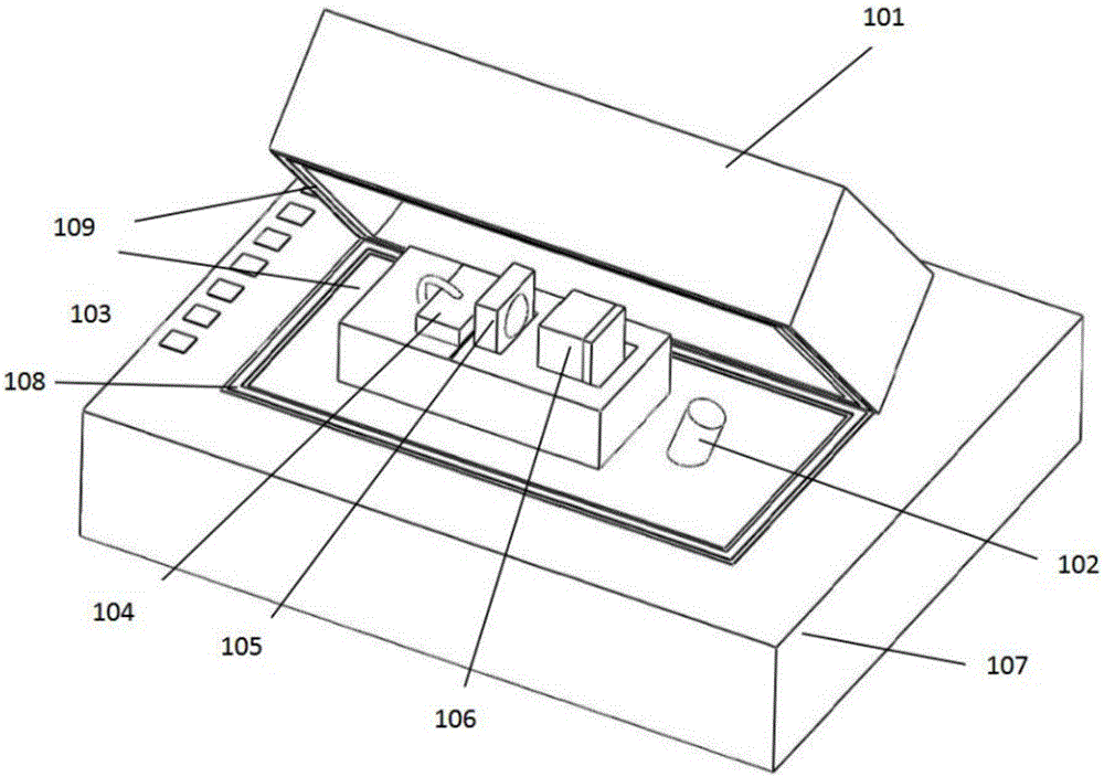
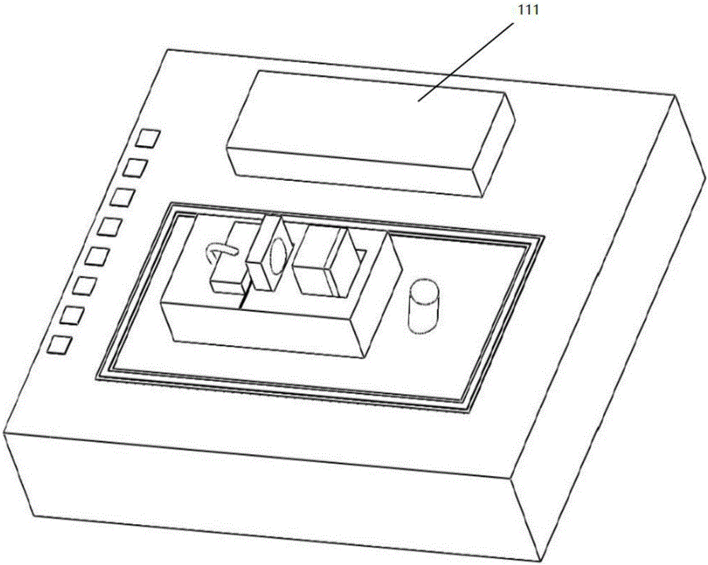
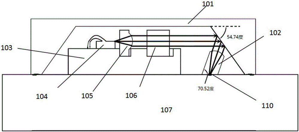
[0041]The device of the present invention includes a sealed box cover 101, a C lens 102, a silicon-based heat sink 103, a laser chip 104, a collimator lens 105, an isolator assembly 106, and a silicon photonic chip 107; wherein, the laser chip 104, the collimator lens 105, the isolation The device assembly 106 is disposed on the silicon-based heat sink 103 , and the silicon-based heat sink 103 is disposed on the silicon photonics chip 107 . The silicon photonic chip 107 includes a grating coupler 110, the C lens 102 is bonded on the silicon photonic chip 107 by ultraviolet glue and aligned with the grating coupler 110, the convex side of the C lens 102 is upward, and the lower surface bonded to the silicon photonic chip 107 is polished The angle is 70.52 degrees; the silicon light chip 107 is provided with a square gold-plated layer 108 on the periphery of the silico...


PUM


Abstract

The invention provides a light source packaging structure, and a positioning and coupling method thereof. The light source packaging structure comprises a sealing box cover (101), a C lens (102), a silicon based heat sink (103), a laser chip (104), an isolator assembly (106), and a silicon light chip (107). The laser chip (104), a collimating lens (105), and the isolator assembly (106) are sequentially disposed on the silicon based heat sink (103). The C lens (102) is aligned with the grating coupler (110) of the silicon light chip (107) in a fixed and coupled manner. The sealed box cover (101) is provided with an inclined inner wall used to reflect light emitted by the laser chip (104) to the C lens, and the lower surface of the C lens (102) is provided with a polishing surface matched with the incident angle of the reflected light. The side of the C lens (102) inclined toward the direction away from the silicon based heat sink (103), and the optical axis of the C lens (102) is consistent with the transmission direction of the light, and the main light is superposed with the optical axis. A coupling structure is compact, and position tolerance is large.

Description

technical field [0001] The invention relates to a packaging method and structure for a silicon photonic chip, in particular to a light source packaging structure of a silicon photonic chip based on a grating coupler and its positioning and coupling methods. The invention belongs to the technical field of optoelectronic integrated devices. Background technique [0002] Optical fiber communication has brought revolutionary development to the transmission of information, and optoelectronic devices in optical fiber communication are also developing in the direction of smaller, more integrated, and cheaper. Optoelectronic integrated chips are one of the research hotspots of optoelectronic devices. Integrated circuit chips are generally manufactured on silicon chips using complementary metal-oxide-semiconductor integration technology, which already has a very mature manufacturing process. Now some manufacturers make waveguides on the top of silicon-based substrates for optical tran...

Claims


Application Information

Patent Timeline
Patent Type & Authority Applications(China)
IPC IPC(8): G02B6/42
CPCG02B6/4214G02B6/4215G02B6/4244G02B6/4251G02B6/4272G02B6/4296
Inventor 石川常进林谦江雄
Owner GUANGXUN SCI & TECH WUHAN
Why Eureka
Try Eureka